


Siemens EDA, "In the 'AI-Native Era,' AI Designs and Verifies Itself"
 Published2026.08.11 16:51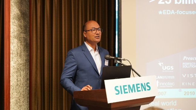
단순 설계 지원 도구서 자율적 작업·결과까지 검증하는 지능형 시스템 진화
AI 에이전트 추론 능력뿐 아니라 툴 호출 신뢰성·보안·토큰 비용까지 최적화
“지멘스 EDA의 ‘AI-Native Design’은 더 빠른 엔진과 에이전틱 AI 기반의 스마트한 실행을 통해 반도체 설계 시간을 단축하면서도, 물리 기반 EDA 엔진으로 정확성을 확보해 반도체 개발 속도와 생산성을 함께 높이겠다”
지멘스 EDA는 11일 서울 잠실 롯데호텔에서 열린 Siemens EDA Forum Seoul 2026에서 차세대 반도체와 시스템 설계 전략을 공개했다.
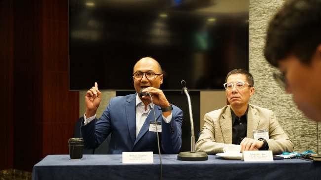
이날 기자간담회에 참석한 앵커 굽타(Ankur Gupta) 지멘스 EDA IC 제품 부문 수석 부사장은 AI 시대의 EDA 시장을 움직이는 핵심 흐름으로 ‘AI 에브리웨어’, ‘소프트웨어 정의 기반 시스템’, ‘이종 통합’, ‘지속가능성’을 꼽았다.
AI 가속 기능이 다양한 칩으로 확산하는 가운데 하드웨어와 소프트웨어의 공동 설계가 중요해지고, 서로 다른 공정과 기능의 다이를 하나의 첨단 패키지에 결합하는 방식도 보편화하고 있다는 설명이다.
고성능 AI 칩과 데이터센터의 전력 소비가 증가하면서 전력 효율 역시 설계 초기부터 고려해야 할 핵심 조건이 됐다.
이 같은 변화는 EDA가 처리해야 할 설계 변수와 검증 작업을 크게 늘린다.
첨단 반도체에서는 작은 오류 하나도 칩의 실패나 수율 저하로 이어질 수 있다.
설계 속도를 높이면서 반도체 물리 법칙에 부합하는 신뢰도 높은 결과를 확보해야 하는 이유다.
앵커 굽타 부사장은 이에 대응하는 AI 네이티브 전략을 ‘더 빠른 엔진’, ‘더 스마트한 실행’, ‘신뢰할 수 있는 결과’라는 세 축으로 정리했다.
AI 네이티브의 핵심은 기존 EDA 엔진을 단순히 생성형 AI와 연결하는 데 그치지 않는다.
여러 AI 에이전트가 설계와 검증 작업을 나눠 수행하고, 물리 기반 EDA 엔진을 ‘사실의 기준’으로 삼아 결과를 스스로 확인하고 오류를 수정하는 구조다.
엔지니어가 퇴근 전 작업 목표를 자연어로 입력하면 에이전트들이 밤새 라이브러리를 특성화하고, 결과를 검증한 뒤 문제를 디버깅하고 수정하는 장시간 자율 워크플로가 대표적인 사례다.
이를 위한 중심 플랫폼이 ‘Fuse EDA AI Agent’ 시스템이다.
지멘스 EDA는 엔비디아의 Nemotron 모델과 NeMo Gym, OpenShell 보안 런타임, CUDA-X 가속 컴퓨팅을 Fuse 및 자사 EDA 엔진과 결합했다.
AI 에이전트의 추론 능력뿐 아니라 툴 호출의 신뢰성, 보안, 토큰 비용까지 함께 최적화하겠다는 구상이다.

특히 Solido 기반 라이브러리 특성화 워크플로에서는 처리 시간을 10배 이상 단축하고 토큰 비용을 5∼10배 절감했다고 밝혔다.
특정 AI 모델에 종속되지 않는 개방성도 강조했다.
앵커 굽타 수석 부사장은 “모델 생태계가 매우 빠르게 바뀌고 있어 하나의 모델에 전념하면 오히려 혁신 속도가 느려질 수 있다”고 설명했다.
Fuse는 EDA 엔진과 AI 모델, 개발 환경을 연결하는 계층으로 설계돼 고객이 엔비디아 Nemotron뿐 아니라 OpenAI, Google, Anthropic 모델 등을 선택할 수 있다.
기업 내부의 데이터와 모델을 활용하는 ‘Bring Your Own Model’ 방식과 온프레미스 운영도 지원한다.
AI 에이전트는 반도체 설계의 최대 병목 가운데 하나인 검증에도 투입된다.
Questa One Agentic Toolkit은 계획 수립, RTL 코드 작성, 린트, CDC, 디버깅, 회귀 테스트 등에 특화된 에이전트를 제공한다.
미디어텍은 엔지니어가 기존에 수주간 교육받아야 했던 작업을 수시간 만에 익힐 수 있었다고 평가했다.
Questa와 Tessent를 결합한 ATPG 시뮬레이션은 기존 대비 3∼5배 빠른 결과를 제공하며, 지멘스 EDA는 장기적으로 10배 가속을 목표로 하고 있다.
AI 네이티브 전략의 범위는 개별 칩을 넘어선다.
지멘스 EDA는 AI 에이전트 기능을 Catapult, Questa One, Veloce, Aprisa, Solido, Calibre, Tessent, Xpedition 등 IC와 PCB 포트폴리오 전반으로 확대하고 있다.
여기에 패키지와 보드, 기계적 응력 및 열 시뮬레이션, 제품 수명주기 관리 기술을 연결해 ‘칩에서 시스템까지’ 이어지는 디지털 스레드를 구축한다는 계획이다.
3D IC에서는 전기적 검증뿐 아니라 열과 응력 같은 멀티피직스 분석이 중요해지는 만큼 종합 산업 소프트웨어 기업이라는 강점을 활용하겠다는 전략이다.
앵커 굽타 수석 부사장은 한국을 메모리와 AI 칩, 가속기 설계를 선도하는 시장으로 평가했다.
지멘스 EDA는 한국에서 인력을 계속 충원하는 한편 AI 설계, 3D IC, 소프트웨어 정의 시스템을 주요 성장 분야로 보고 있다.
앵커 굽타 수석 부사장은 “AI 네이티브 EDA가 지향하는 것은 엔지니어를 대체하는 자동화가 아니라 반복적인 실행 부담을 AI에 맡기고, 엔지니어가 더 많은 시간을 구조적 혁신과 설계 판단에 투입하도록 하는 것”이라며 “설계 속도와 생산성, 결과 신뢰성을 동시에 끌어올리는 능력이 앞으로 EDA 시장의 경쟁력을 가를 것”이라고 밝혔다.

Comments
Related news
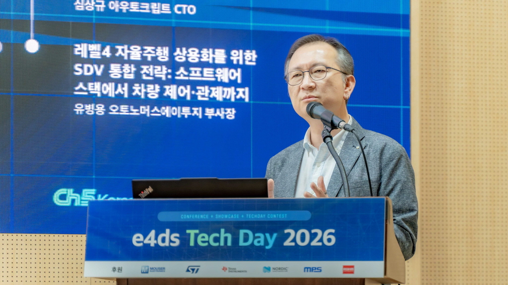
[e4ds Tech Day 2026 ⑨] Sim Sang-gyu, Autocrypt CTO: "In the Physical AI Era, Automotive Security Must Extend Beyond the Vehicle"
At e4ds Tech Day 2026, Sim Sang-gyu, CTO of Autocrypt, explained automotive cybersecurity strategies in the era of Physical AI and SDV (Software-Defined Vehicle). Automobiles are evolving as part of an ecosystem connected to AI, cloud, chargers, IoT, and robots, and he emphasized that the scope of security must expand beyond the vehicle interior to the entire connected environment. In particular, AI model tampering, adversarial attacks, OTA updates, and EV charger hacking were identified as major threats. He explained that response measures require zero trust, AI model integrity protection, intrusion detection, Security by Design and Default, and full lifecycle security management, and that proactive security system establishment beyond regulatory compliance is critical for securing future mobility competitiveness.
2026.10.12by 배종인 기자

Practical HIL Construction Strategy for Automotive and Off-Highway Controller Validation
As vehicle E/E architecture transitions to zonal structures and shifts to software-defined vehicles (SDV), the number of controllers (ECUs) requiring validation and software complexity are surging dramatically. Meanwhile, real vehicle testing cannot provide repeated verification under identical conditions and entails lead time and safety concerns. This white paper explains the principles of HIL (Hardware-in-the-Loop) validation and the structure of the NI platform composed of PXI, SLSC, and VeriStand, and through two actual implementation cases—Camera Record & Replay HIL for In-Cabin Monitoring Controller (ICMU) and Forklift Controller (VCU) HILS—describes how controller-level regression testing becomes possible. Additionally, it explicitly states application boundaries and limitations, such as lack of A2B support.
2026.10.12by 편집부
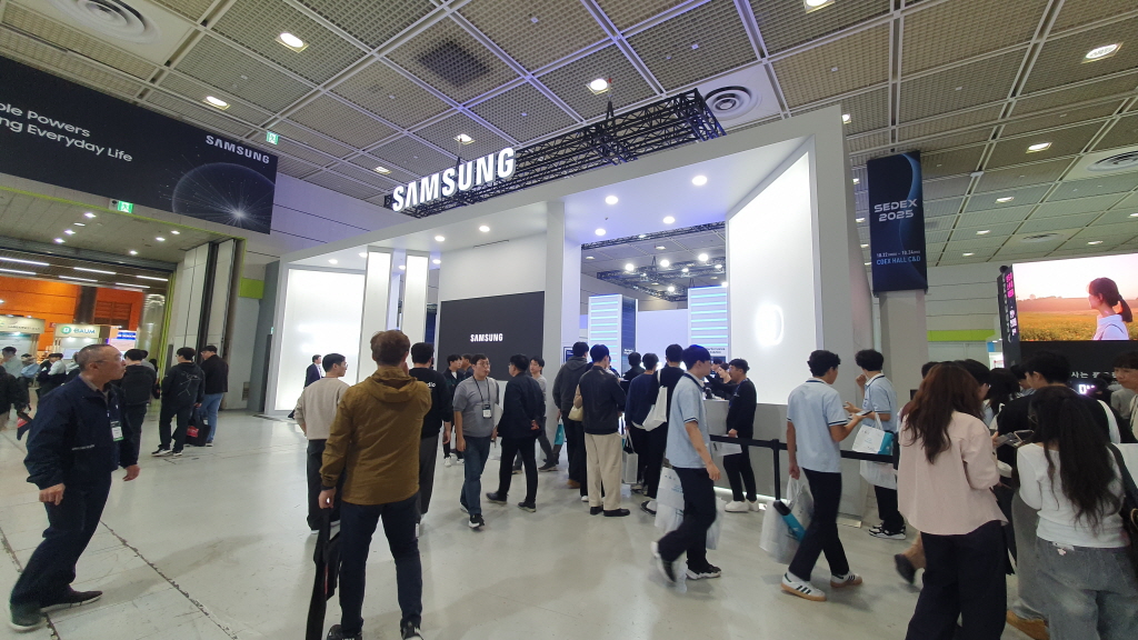
SEDEX 2026 Opens…Largest Semiconductor Exhibition Ever Showcasing AI Memory and Physical AI
The Korea Semiconductor Industry Association (KSIA) will host SEDEX 2026, a specialized exhibition for semiconductor materials, components, and equipment, over three days from October 14-16 at Seoul COEX. Domestic and international semiconductor-related companies will participate to showcase the latest technologies and products while creating opportunities to strengthen supply chain cooperation.
2026.10.12by 배종인 기자
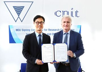
Korea Automotive Research Institute Signs MOU with Italy National Institute for Wireless Communications
The Korea Automotive Research Institute will sign an MOU with Italy's National Institute for Wireless Communications and launch joint research on next-generation mobility technologies based on 6G, V2X, and connected vehicles. The two organizations will conduct research to apply advanced wireless communication technologies to vehicles and discover international joint projects to advance next-generation connected vehicle technology development.
2026.10.12by 배종인 기자
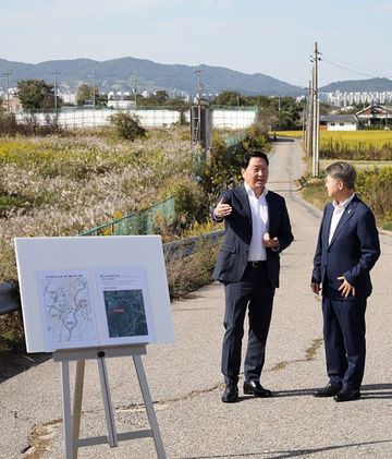
SK Group Chairman Choi Tae-won Directly Inspects Gwangju Semiconductor Cluster Site
SK Group Chairman Choi Tae-won directly inspected the planned semiconductor specialized complex site in Jeollanam-do·Gwangju Integrated Metropolitan City, demonstrating his determination to accelerate the creation of a 400 trillion won-scale Honam region cluster. As demand for AI memory semiconductors surges and the Yongin cluster construction schedule was shortened by 12 years yet is still expected to be insufficient, SK Hynix plans to construct factories concurrently in both Yongin and Jeollanam-do·Gwangju.
2026.10.12by 배종인 기자











