



The Future Opened by the Convergence of Light and Semiconductors…'Optical Science and Optical Semiconductor Workshop 2026' Held in Suwon
 Published2026.08.21 09:55
imec 신동재 박사·연세대 최우영 교수 기조 발표
PIC부터 첨단 패키징까지 8개 분야 집중 조명
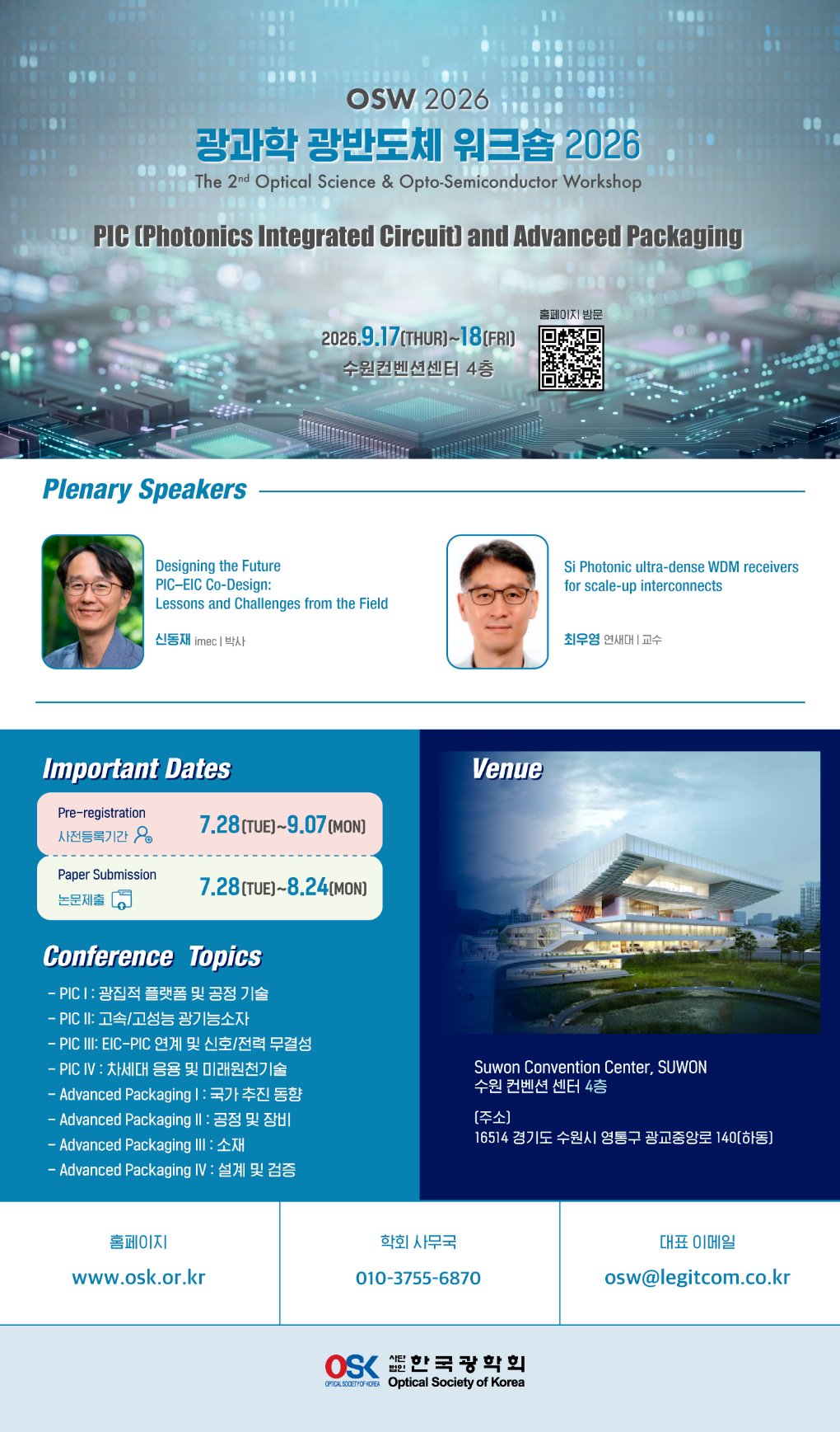
사단법인 한국광학회는 오는 9월 17일부터 18일까지 수원컨벤션센터 4층에서 ‘제2회 광과학 광반도체 워크숍 2026(OSW 2026)’을 개최한다. 올해 워크숍의 중심 주제는 ‘광집적회로와 첨단 패키징(PIC and Advanced Packaging)’이다.
광집적회로, 즉 PIC(Photonics Integrated Circuit)는 빛의 생성과 변조, 전송, 검출 등에 필요한 여러 광학 기능을 하나의 칩에 집적하는 기술이다.
인공지능 데이터센터와 초고속 통신 시스템의 성능이 빠르게 높아지면서 대용량 데이터를 낮은 전력으로 전송할 수 있는 광반도체 기술의 중요성도 함께 커지고 있다.
이번 워크숍은 광과학과 반도체, 패키징 분야의 연구자와 산업계 전문가가 최신 기술을 공유하고 협력 가능성을 논의하는 전문 학술 교류의 장으로 마련된다.
기조 발표에는 세계적인 반도체 연구기관 imec의 신동재 박사와 연세대학교 최우영 교수가 나선다.
신동재 박사는 ‘미래를 설계하는 PIC-EIC 공동설계: 현장의 교훈과 과제(Designing the Future PIC-EIC Co-Design: Lessons and Challenges from the Field)’를 주제로 발표한다. 광집적회로인 PIC와 전자집적회로인 EIC를 하나의 시스템 관점에서 공동 설계하는 과정에서 얻은 경험과 기술적 과제를 소개할 예정이다.
PIC와 EIC의 공동설계는 광소자와 전자회로를 각각 개발한 뒤 결합하는 방식에서 벗어나 초기 설계 단계부터 두 회로의 성능과 연결 구조를 함께 고려하는 접근이다. 고속 신호 처리와 소비전력 절감, 시스템 집적도 향상을 위해 중요성이 커지는 분야다.
최우영 연세대학교 교수는 ‘확장형 인터커넥트를 위한 실리콘 포토닉 초고밀도 WDM 수신기(Si Photonic ultra-dense WDM receivers for scale-up interconnects)’를 발표한다.

여러 파장의 빛에 각각 데이터를 실어 보내는 파장분할다중화(WDM) 기술과 실리콘 포토닉 수신기를 활용해 시스템 내부 연결의 데이터 처리 능력을 확장하는 기술을 다룬다.
이번 기조 발표는 광반도체 기술이 개별 광소자의 성능 향상을 넘어 전자회로와의 공동설계, 초고밀도 광연결, 시스템 확장성 확보로 발전하고 있음을 보여줄 것으로 기대된다.
주요 학술 발표는 PIC 분야와 첨단 패키징 분야로 나뉘어 진행된다.
PIC 분야에서는 먼저 ‘광집적 플랫폼 및 공정 기술’을 다룬다. 광집적소자를 구현하기 위한 기반 플랫폼과 제작 공정에 관한 연구가 주요 대상이다. ‘고속·고성능 광기능소자’ 분야에서는 빠른 데이터 전송과 효율적인 광신호 처리를 위한 핵심 소자 기술이 소개된다.
‘EIC-PIC 연계 및 신호·전력 무결성’ 분야도 주요 주제로 제시됐다. 전자집적회로와 광집적회로를 연결할 때 발생할 수 있는 신호 손실과 전력 공급 문제를 다루는 분야다. 이와 함께 ‘차세대 응용 및 미래 원천기술’ 발표를 통해 광통신과 인공지능 시스템 등으로 확장될 광집적 기술의 발전 방향을 살펴본다.
첨단 패키징 분야에서는 국가별 기술개발 및 산업 추진 현황을 살펴보는 ‘국가 추진 동향’ 세션이 마련된다. 반도체 패키징을 실제로 구현하기 위한 ‘공정 및 장비’, 고성능 패키지의 기반을 이루는 ‘소재’, 제품의 신뢰성과 완성도를 좌우하는 ‘설계 및 검증’도 주요 발표 분야에 포함됐다.
광반도체가 실제 시스템에 적용되려면 우수한 광소자만으로는 충분하지 않다. 광소자와 전자소자를 정밀하게 배치하고 연결하는 패키징 공정, 신호와 전력을 안정적으로 전달할 구조, 열과 소재 특성을 고려한 설계 및 검증 기술이 함께 뒷받침돼야 한다. 이번 워크숍이 PIC와 첨단 패키징을 하나의 주제로 묶은 배경도 이러한 기술적 연계성에 있다.
논문 제출 기간은 7월 28일부터 8월 24일까지다. 사전등록은 7월 28일부터 9월 7일까지 진행된다. 행사장은 수원시 영통구 광교중앙로 140에 위치한 수원컨벤션센터 4층이다.

Comments
Related news
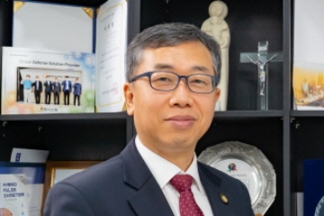
[Interview] Kim Jang-sun, CEO of Panoptics - “We will become a global leader in optical communications and optical sensors”
We arranged an interview with Kim Jang-seon, CEO of Panoptics, a specialized company in optical communications, terahertz, laser, and IoT fields, to learn about Panoptics' core technologies, products, and future strategies.
2022.01.19by 성유창 기자

Arm Announces CPU Benchmarking Methodology for Agentic AI
Arm has announced a CPU performance evaluation methodology specialized for agentic AI workloads. Developed with support from Fujitsu, Meta, and OpenAI, this methodology focuses on performance measurement based on actual agent task completion results. According to independent verification by Signal65, the Arm AGI CPU demonstrated an average performance advantage of 1.99x per rack compared to AMD EPYC Turin, with performance differences of 1.7x to 2.2x particularly in the tooling, orchestration, and inference domains.
2026.10.15by 배종인 기자
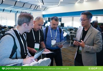
Panasia Accelerates CXL Appliance Deployment at OCP Global Summit 2026
Panasia unveiled a complete CXL server rack solution based on PCIe 6.4-CXL 3.2 fusion switch technology at OCP Global Summit 2026. As memory demand increases with the proliferation of agentic AI, Panasia's solution integrates CPU, memory, and accelerators into a single fabric, enabling large-scale CXL environments to be configured without separate testing. Hyperscalers have reported results of reducing server counts by up to 25% through CXL memory deployment, and Panasia expects to accelerate the timeline for datacenter CXL adoption through collaboration with major system manufacturers.
2026.10.15by 배종인 기자
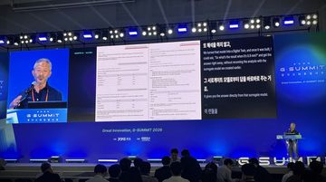
SiHighSys partners with Gyeonggi-do fabless companies at G-SUMMIT 2026
SiHighSys participated in G-SUMMIT 2026 alongside four Gyeonggi-do fabless startups, operating a joint booth, hosting presentation sessions, and organizing startup meetups. The company introduced the impact of agentic AI on product design and verification through AI simulation technology as a common ground, and presented methods to reduce development time and costs through the convergence of simulation and AI. The company supported domestic startups' global market expansion while exploring technical collaboration opportunities.
2026.10.15by 배종인 기자
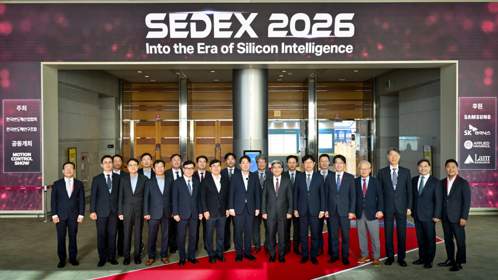
SEDEX 2026 Opens...Keynote and VIP Tour Held
The Korea Semiconductor Industry Association-organized semiconductor equipment and materials specialist exhibition 'SEDEX 2026' officially opened on the 14th. Operating without a separate opening ceremony, the event proceeds with keynote sessions and VIP tours, serving as a venue where domestic and international semiconductor industry supply chain-related companies participate to showcase their technologies and products. The operational approach is characterized by its focus on substantive business exchange.
2026.10.14by 배종인 기자











