


[Technical Contribution] ADI, "Power Sequencing Innovation Possible Without Programming"
 Published2026.09.14 10:08
ADM6840, Sequencing and Monitoring of Up to 8 Voltage Rails Using Only Resistors and Capacitors
Enables Highly Reliable Power Management Design Without Auxiliary Power Supply or Programming
■ Overview
This article explains the necessity of power sequencing required by various digital loads and discusses several methods for implementing power sequencing and voltage monitoring functions.
Additionally, it introduces a new concept of user-friendly power sequencing solution that requires no programming, digital communication, or separate bias power supply.
These characteristics of the new solution are very important because the power sequencer must be the first device to operate in the system.
At the time when the sequencer first operates, the digital devices that can communicate with the sequencer are generally not yet activated.
■ Introduction
Electronic loads such as FPGA, GPU, CPU, DSP, and SoC require power sequencing.
That is, different supply voltages must rise and fall in a predetermined sequence.
If proper power sequencing is not performed, the functionality of the load may be limited or malfunctions may occur.
In severe cases, these loads may be damaged.
Power sequencing functions are used to prevent such problems.
■ Power Sequencing Examples
Generally, a circuit can be used in which the voltage generated from each voltage converter is connected to an enable pin so that multiple voltage converters are turned on sequentially.
However, this approach requires voltage converters with precisely defined threshold values for enable pins, and it is difficult to implement individual voltage rail power turning off in a specific sequence.
In addition, complex additional circuitry is required for precise time control of power on and off.
This is why dedicated power sequencing controller usage is preferred.
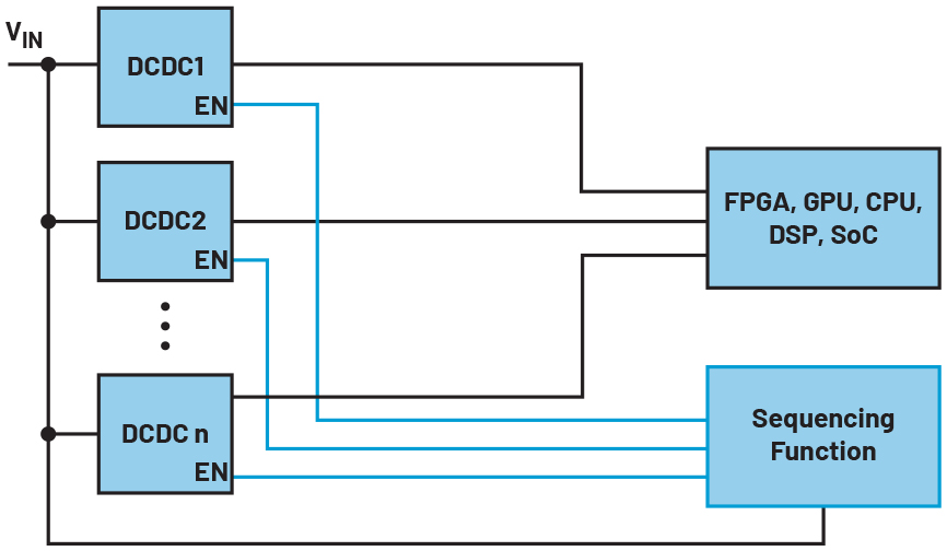
Figure 1 shows the basic structure of such a system. By controlling the enable pin of each voltage converter, the sequencer ensures that the voltage converters DCDC1 through DCDCn turn on and off in the correct order.
It is desirable for such power sequencing devices to support as wide a universal input voltage range as possible.
Since the sequencer must operate before each power rail in the system is applied, a wider input voltage range makes it easier to apply to various systems.
Power sequencing functions can be composed of various functional blocks.
For example, these functions can be implemented using a microcontroller (MCU), a small FPGA, a dedicated sequencer with programmable memory, or a simple power sequencer.
However, each of these solutions has its own limitations. An MCU must start operating first and execute a pre-written program.
Small FPGAs and sequencers with programmable memory must also be programmed before use.
This process can be performed before mounting the component on the PCB or before applying initial power after mounting.
Both methods require considerable effort and cost.
■ Power Sequencing Solution
To solve these problems, a sequencing solution has been developed that requires no separate programming during production.
This solution can set sequencing operation using only resistors and capacitors, making implementation simple.
Additionally, this sequencer supports a very wide input voltage range of 2.7V to 15V and can be directly driven by 3.3V, 5V, or even 12V power supplies without a separate power supply for the sequencer itself.
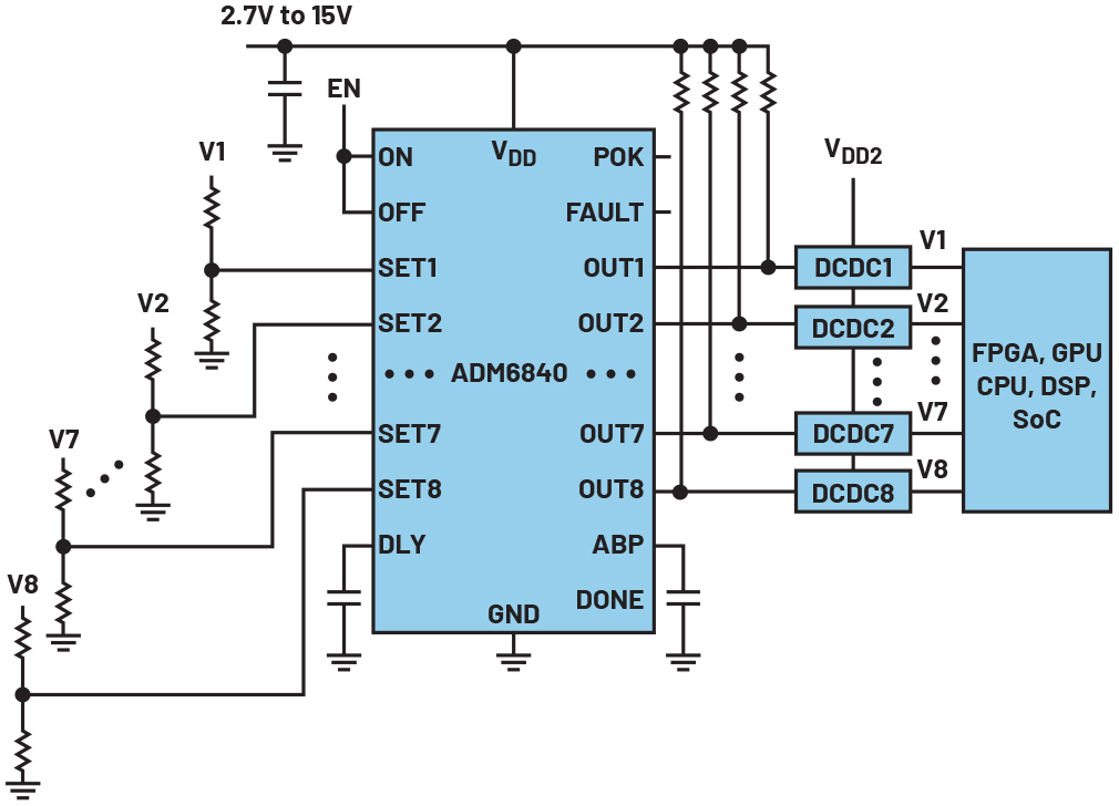
As can be seen in Figure 2, this solution provides another useful function in addition to the power sequencing function.
It individually monitors each voltage from V1 to V8 and outputs a 'Power OK' signal only when all voltages reach preset values.
The accuracy of voltage monitoring is very important.
Monitoring accuracy is one of the key factors determining the overall accuracy of each voltage generated by the DC-DC converter. The ADM6840 provides high voltage monitoring accuracy of ±0.8%.
To reliably protect the circuit, it is important that the monitoring module operates reliably.
Additionally, since many circuits operate in high-temperature environments, the ADM6840 supports a wide operating temperature range of -40°C to +125°C.
When controlling more than 8 power rails, multiple sequencers can be used together.
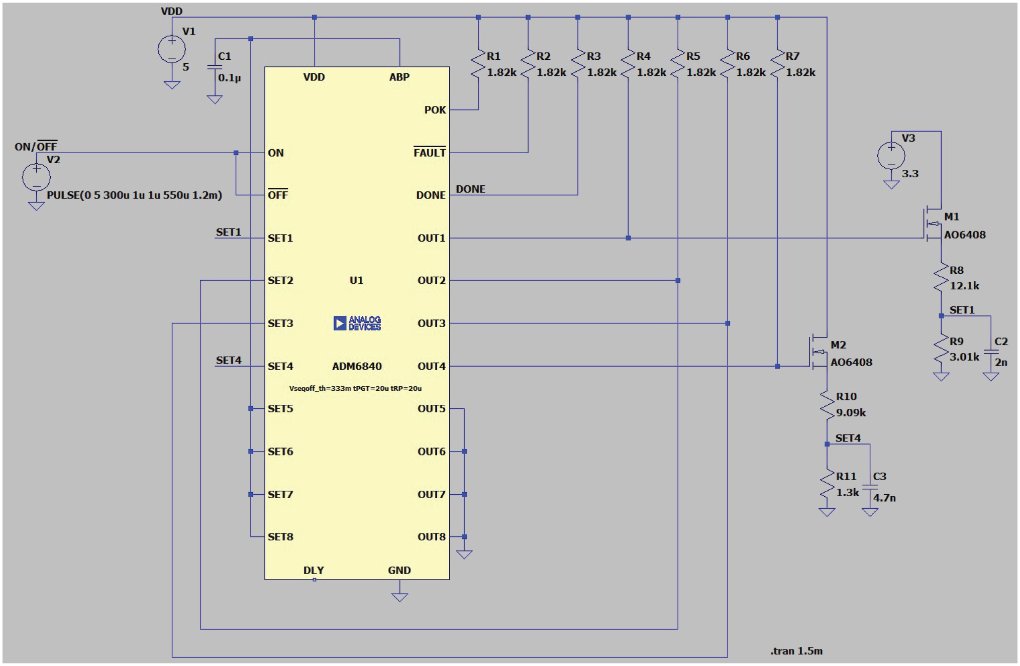
LTspice®, a free simulation software tool, is provided to easily evaluate the functionality of the ADM6840 sequencer.
LTspice includes example circuits using the ADM6840 sequencer. Figure 3 shows a simulation environment where different settings can be simulated.
■ Conclusion
Sequencing functions can be implemented very easily by utilizing appropriate functional blocks.
In most applications, no separate auxiliary power supply is required, and time-consuming programming processes are also unnecessary.
Therefore, a highly reliable power sequencing system can be designed within a short development period.
※ Author Profile
Frederik Dostal is a power management specialist with more than 20 years of experience. After majoring in microelectronics at the University of Erlangen in Germany, he joined National Semiconductor in 2001 and worked as a field application engineer, gaining experience in implementing power management solutions in customer projects. During his tenure at NS, he worked for 4 years in Phoenix, Arizona, as an application engineer responsible for switch-mode power supplies (SMPS). Since joining Analog Devices in 2009, he has performed various roles including product line management and European technical support. Currently, he works as a power management specialist based on extensive design and application experience. He is currently working at Analog Devices' Munich office.
Comments
Related news
[Technical Contribution] ADI Develops Scalable Beamforming Engine for Quad-Apollo MxFE Radar and Communications Systems
We spoke with Siddhartha Das, System Applications Engineer at Analog Devices, Inc., about how Analog Devices' Apollo MxFE-based digital beamforming platform implements a phase-coherent, scalable direct RF sampling architecture for next-generation radar and communication systems.
2026.01.12by 명세환 기자
ADI, “Innovation to Simplify Power Compensation Evaluation Using Software-Based Compensation Probes”
We spoke with Frederik Dostal, a power management expert at Analog Devices, Inc., about a simplified method for evaluating power supplies with different compensation settings applied.
2026.05.19by 편집부

ADI Strengthens AI Power Semiconductor with Acquisition of Empower
Analog Devices (ADI) is acquiring Empower Semiconductor for $1.5 billion to expand its power management portfolio for AI data centers. The acquisition is interpreted as a strategic move to secure processor-adjacent power conversion technology, amid rising design challenges in power density and thermal management in AI servers and accelerators.
2026.05.21by 배종인 기자

Resolving a single robot with 11 ICs… Marknica Korea’s ADI Integrated Solution
The market for industrial robots and collaborative robots, as well as mobile robots represented by AMRs and AGVs, is growing rapidly domestically. As the government launches the K-Humanoid Alliance in April 2025 and commits to investing over 1 trillion won in humanoids by 2030, logistics automation and collaborative robot adoption are simultaneously increasing in industrial settings, leading to active entry of new robotics startups. Within this trend, the first question robot developers face is surprisingly straightforward: what components should be used to build robots. Stable power supply, precise motor control, stable pose recognition, and increasingly important Edge AI—the ICs that go into a single robot are diverse in type and have demanding requirements. At Makrenica Korea, the official Korean distributor of Analog Devices (ADI), Park Sang-kwon, a FAE responsible for technical support, discussed the message to be covered in ADI's upcoming robotics integrated solutions webinar. Park, a general FAE who supports various fields, noted that robotics is the field where inquiries have been increasing most rapidly in recent times.
2026.06.03by 명세환 기자
ADI Supports NVIDIA MGX-Based AI Data Center 800VDC Power Architecture
Analog Devices (ADI) is supporting the adoption of 800VDC power architecture in AI datacenters based on the NVIDIA MGX architecture by providing power technologies, thereby responding to the transformation of AI datacenter power infrastructure.
2026.06.08by 배종인 기자











