



ASM launches PECVD-based 'Flowable Carbon' technology
 Published2026.09.30 08:58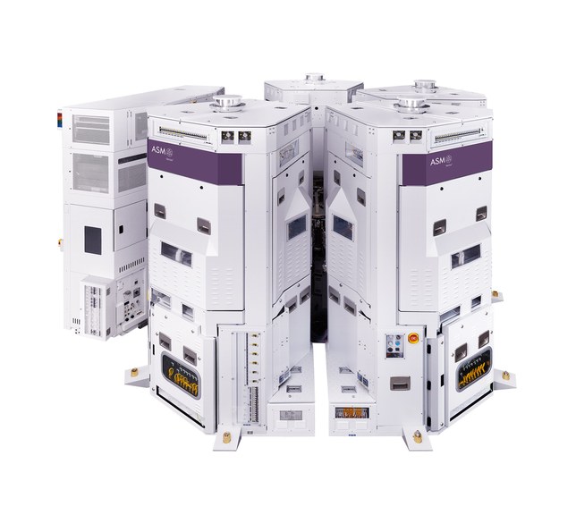
It is the first instance of simultaneously implementing gap fill and planarization in a single PECVD process, integrating processes that previously proceeded in multiple steps into a single platform.
It is currently being applied in early mass production.
Since it is implemented in an all-in-one PECVD system, there is no need to undergo CMP (chemical mechanical planarization) or etch-back processes in subsequent steps, the company added.
The company explained that planarization levels can be improved even on substrates with varying pattern densities, providing scalability to address current and future technology nodes.
ASM is a semiconductor wafer process equipment company headquartered in the Netherlands, and operates an R&D center and manufacturing facility in Dongtan, Hwaseong, Gyeonggi.

Comments
Related news
ASM, $100 million investment in Mars 2nd Manufacturing Research Innovation Center begins in earnest
ASM, a global semiconductor company from the Netherlands, is investing $100 million in Hwaseong, Gyeonggi Province, to expand its R&D and manufacturing facilities, and is entering full-scale operations to expand the supply of PEALD used in advanced semiconductor processes.
2023.05.23by 배종인 기자
MathWorks Releases MATLAB·Simulink R2026b
MathWorks released MATLAB·Simulink R2026b on the 30th. New features including Simulink Variant Manager, Visual Inspection Toolbox, and Polyspace Test Server have been added, and 10 toolboxes have been updated. The release supports the entire process from design of complex systems combining software, AI, and electronics to verification and deployment, enabling organizations to simultaneously achieve development speed, quality, and regulatory compliance.
2026.09.30by 배종인 기자
Applied Materials and KIOXIA to Co-develop Next-Generation Memory at EPIC Center
Applied Materials and KIOXIA are undertaking joint development of next-generation memory for AI at the EPIC Center in Silicon Valley. The two companies will collaborate across all areas from memory cell structure formation through multichip stacking, advanced packaging, and materials engineering innovation, with the goal of enhancing memory density and performance required for AI infrastructure. The EPIC Center, a $5 billion-scale R&D facility, is slated to commence operations within the year.
2026.09.30by 배종인 기자
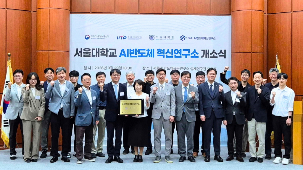
Seoul National University launches AI Semiconductor Innovation Institute...fostering 110 AI semiconductor talent through industry-academia collaboration
Seoul National University held an opening ceremony for the 'AI Semiconductor Innovation Institute' on the 29th at Doyeon Hall in the Design Research Building of the Semiconductor Joint Research Institute and commenced full-scale operations.
2026.09.30by 배종인 기자
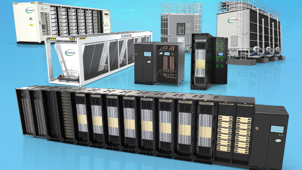
Supermicro Begins Shipping NVIDIA Vera Rubin NVL72 Racks
Supermicro has begun shipping NVIDIA Vera Rubin NVL72 racks. Integrating DCBBS and DLC-2 liquid cooling technology, the product supports 1,152 GPUs and 331TB of HBM4 memory per single scalable unit. By pre-validating the entire cooling system from cold plates to cooling towers and supplying it, customers can immediately deploy end-to-end integrated complete systems in production environments.
2026.09.29by 배종인 기자











