This white paper examines the challenges faced when attempting to meet the performance requirements of next-generation systems with existing FPGAs and introduces Altera's new core architecture known as HyperFlex™. This new HyperFlex architecture, combined with Intel's 14nm Tri-Gate process technology—exclusively available to Altera—enables Stratix® 10 FPGAs and SoCs to achieve levels of performance and power efficiency unimaginable in previous generations of high-performance FPGAs. The features enabled by these devices are as follows:
- Doubled core performance and more than 5 times higher integration density compared to the previous generation Stratix V FPGA
- Up to 70 percent less power consumption than Stratix V FPGAs at the same performance
- Built-in quad-core 64-bit ARM® Cortex®-A53 hard processor system (SoC version)
Industry challenges
Electronic system developers in all major industrial sectors are facing a situation where they must continue the fierce rate of increase they have achieved over the past few decades. Customers in various markets, such as military communications and computer storage environments, not only want faster systems but also want systems that are smaller in size and consume less electricity.
However, the demand for speed is nothing new. What is changing is that the requirements in the wired and wireless, military, broadcasting, computing, and storage sectors are becoming even more demanding. In many fields, these demands are showing high double-digit growth rates reminiscent of a boom period.
[Figure 1] Customer demand in application fields such as wired, wireless, and data centers is increasing.
The information and communications technology (ICT) sector is a prime example of a field where customer demands are challenging the capabilities of the system developers and semiconductor suppliers that support them. Due to the trend of massive amounts of data traversing global networks, the scale of global bandwidth consumption is doubling every two to three years. In 2016, data equivalent to the total volume of all movies ever produced will be transmitted in all directions through these networks every three minutes. TeleGeography (1), a market research firm, stated that internet bandwidth more than doubled during the period from 2010 to 2012, soaring to 77 terabits per second.
As everything from automobiles and industrial equipment to home appliances such as refrigerators becomes connected to the Internet, the demand for communication capabilities will skyrocket. Gartner predicts that the number of Internet of Things (IoT) devices will increase nearly 30-fold from 900 million in 2009 to 26 billion in 2020.(2)
Many trends are contributing to this endless increase in bandwidth. For example, while 100 gigabits per second (Gbps) Ethernet has only just begun to replace the currently widely used 40 Gbps version, the IEEE has recently established a dedicated department to pursue a 400 Gbps standard.(3)
Although wired networks still transmit the most data, the wireless market is attempting to reverse this trend. According to a report by Cisco, wired devices accounted for nearly 55 percent of IP traffic in 2011. However, given the explosive growth of smart mobile devices, it is easy to predict that wireless devices will soon become the mainstream of traffic. Cisco predicts that the volume of mobile data traffic will skyrocket from 1.6 exabytes in 2013 to 11.2 exabytes in 2017.(4)
As other fields are also showing tremendous double-digit growth rates, the need for faster data processing equipment is becoming even greater. Although satellite communications are still predominantly used for military purposes, traffic is skyrocketing as drones and satellites generate more data and are used by far more people than in the past. This is causing the requirements for ground backhaul stations to rise rapidly.
Northern Sky Research (NSR) predicts that the global installed base of satellite backhaul sites will increase by more than 50 percent between 2012 and 2022. (5) This increasing trend is driven by the need to cost-effectively meet the 3G/4G/LTS backhaul requirements of mobile carrier customers. NSR predicts that the demand for total transmission capacity of high throughput satellites (HTS) will increase by 133.5 Gbps in the backhaul service sector alone by around 2022. According to NSR's forecast, more than 4.3 million new subscribers will be added to the global satellite broadband access market over the next decade, and nearly 2.4 million new subscribers will be added in North America by around 2022.
On the ground, the mobile communications sector is driving the demand for faster chips and systems. According to Cisco's forecast, mobile traffic volume is expected to increase by 78 percent during the period 2011–2016. A significant portion of this is driven by video, which is projected to show an annual growth rate of 90 percent during the 2011–2016 period. Cisco anticipates that by around 2016, mobile video will account for more than 70 percent of total mobile data traffic.(6)
Public demand for video is also triggering strong growth in the broadcasting industry. Most countries are expected to complete the transition to digital TV by around 2019. Additionally, the growth of HDTV and the emergence of Ultra High Definition (UHD) technology are expected to create a need for faster editing and transmission systems.
Reduction in power consumption and heat generation
In all these fields, simply designing faster equipment is no longer sufficient. Power consumption has become a critical issue due to concerns about the environment as well as the cost savings associated with energy conservation. For both chip manufacturers and system developers, energy conservation has become a central factor in most projects. For system design teams, the reduction in heat generated by energy conservation is also welcome, as it reduces the time spent on heat dissipation issues.
Data centers can be considered a typical example where power saving and heat reduction are required. According to the 2012 Global Census by Datacenter Dynamics, the power demand of data centers worldwide increased from 24 gigawatts (GW) in 2011 to 38 gigawatts in 2012, showing a growth rate of 63 percent.(7) Many U.S. statisticians cite the research results of Dr. Jonathan Coomey to estimate that data centers consume about 2 percent of electricity usage in the United States.(8)
The Need for a New Approach
Regardless of the industry, next-generation systems are increasingly requiring greater data throughput and higher clock frequency performance. Faced with this reality and the need to launch new products rapidly, numerous companies are currently using FPGAs as a core component of their system designs. The data throughput of these FPGAs is often a critical factor in determining overall system performance.
The most common technique used to improve the data throughput of FPGAs is to progressively widen the on-chip bus. It is common for FPGAs to use buses of 512 bits, 1,024 bits, or even wider. Using such wide buses requires the use of expensive FPGA resources and increases power consumption. Furthermore, it becomes difficult to perform high-speed logic functions, such as comparators or checksums, across every bit of the bus.
In addition to using a wider bus, system developers increase clock frequency through extensive pipelineization of the data path. However, pipelined wide buses require consuming additional FPGA resources for each bit of the bus, which is also costly. Therefore, making the bus width increasingly wider is not practical.
Moving to next-generation technology nodes also brings performance improvements. However, as process geometry continues to shrink, interconnect latency between logic blocks accounts for an increasingly larger proportion of the total latency in FPGAs. This problem is not resolved simply by advancing existing FPGA architectures to next-generation technology nodes. To address this interconnect latency issue, which is becoming increasingly important, a better solution is required.
Achieving performance beyond imagination
The new HyperFlex architecture of the Stratix 10 device is an innovative approach to solving these problems. This architecture provides performance and power efficiency that are impossible to achieve with existing FPGA architectures. By using the new HyperFlex architecture with Intel's 14nm Tri-Gate process technology, developers can double the core performance of Stratix 10 FPGAs and SoCs compared to previous generation high-performance FPGAs.
Benefits of HyperFlex
The key innovations that enable the benefits of HyperFlex are as follows:
Registers omnipresent everywhere
The “registers everywhere” of interconnect wiring are called Hyper-Registers, and these are existing registers included within Adaptive Logic Modules (ALMs).It is distinctly different from the Gisters.
Hyper Register is associated with each individual wiring section within the device and is also provided to the inputs of all functional blocks such as ALM, embedded memory (M20K) blocks and DSP (digital signal processing) .
Programmable clock tree synthesis enables system developers to maximize core clocking performance by generating localized clock trees to reduce skew and timing uncertainty. This capability is one of the key features that allows the HyperFlex architecture to double performance. In addition, core clocking reduces dynamic power consumption of the clock network by utilizing intelligent branch activation features.
Hyper-Aware Design Flow
The three new improvements to the Hyper-Aware design flow are as follows:

- Enables the exploration of performance and guides users to maximize design performance
Fast Forward Compile tool.
- HyperRetimer stage that supports performance optimization after placement and wiring operations.
- Enhanced synthesis, placement, and wiring algorithms using hyper-registers.
Benefits Beyond High Performance
The enhanced core performance of the HyperFlex architecture offers various benefits to system developers, and as shown below, these benefits are not limited to the obvious advantage of being able to execute cores faster.
- Thanks to improved core performance, timing closures can be performed more easily and quickly, so
Design teamProductivity is improved and the product's time-to-market is shortened.
- Improved core performance allows developers to use lower-speed devices while
It enables the reduction of solution costs by exceeding performance requirements.
- Enhanced core performance capable of executing designs at doubled speeds of the original internal bus width
By implementing it at half the size, the overall size of the design can be reduced. Therefore, the design can be much
Solution costs are reduced because it can be fitted into a smaller device.
Intel Advantage
In February 2013, Altera announced that Intel's 14nm Tri-Gate (FinFET) process technology would be used to manufacture the next-generation Stratix 10 FPGAs and SoCs. This technology provides groundbreaking levels of integration, performance, and power efficiency. The 3D FinFET (Tri-Gate) transistors underlying this technology are replacing existing 2D planar MOSFET transistors as the process geometry shrinks to below 20nm. All major silicon foundries have already announced plans to transition to 3D FinFET transistors. By selecting Intel as their foundry partner for Stratix 10 devices, Altera and its customers have been able to enjoy the numerous benefits offered by “The Intel Advantage.” Because of these advantages, Intel's 14nm Tri-Gate technology is an ideal process for implementing the new HyperFlex architecture.
The five best benefits Altera and its customers can gain from their relationship with Intel are as follows:
- Exclusive Rights: Altera is the only major FPGA vendor to access Intel's 14nm Tri-Gate technology
It is a company that can do it. These exclusive rights clearly demonstrate the strong bond between Altera and Intel.
Only Altera's customers can utilize Intel's industry-leading process technology.
- Production Capacity: Other major semiconductor foundries have also announced plans to develop new processes based on FinFET transistors.
However, to implement FinFET technology in production rather than at the laboratory level, one must go through a steep learning curve.
does.
Intel is the only company to have transitioned to the production phase so far, having already produced over 500 million FinFET transistor devices
Shipped.
- A process one step ahead: It has already been over three years since Intel introduced its 22nm Tri-Gate process.
This technology has now advanced to 14 nm and is being used in Altera's Stratix 10 FPGA and SoC.
FinFET processes being developed by other semiconductor foundries will start using the existing 20nm design rule.
Since they are not adopting processes scaled down to the same level as Intel, Intel, which is effectively one process ahead,
It has significant advantages in terms of performance, power efficiency, and integration.
- Maturity: Intel and Altera are using 2nd generation 14nm Tri-Gate technology. On the other hand, among other foundries
No company has announced when it plans to start manufacturing chips using the first-generation FinFET process.
Stratix 10 FPGAs and SoCs benefit from Intel's mature 14nm Tri-Gate process technology.
- Design Expertise: Intel uses FinFET transistors for high-speed logic, analog, digital, and mixed-signal circuits
It has demonstrated that it possesses the capability to design and produce. As such, Altera
Since extensive design expertise is available, Stratix 10 FPGAs and SoCs utilize Intel's 14nm Tri-Gate process
It is possible to make the most of technical capabilities.
Altera can also provide key high-performance FPGA and SoC products that are exclusively produced in the United States through its ties with Intel. This enables access to world-class packaging and assembly capabilities, allowing for the development of heterogeneous multi-die devices that integrate 14nm Stratix 10 FPGAs and SoCs with other advanced components (which may include SRAM, DRAM, ASICs, processors, and analog components) into a single package. These benefits are the “Intel Advantage” available only to Altera’s Stratix 10 FPGA and SoC customers.
HyperFlex Architecture
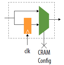
At the heart of the new HyperFlex architecture is an innovative “omnipresent register” design, in which bypassable hyper registers are added to every wiring section and every function block input within the FPGA core. Figure 2 shows a bypassable hyper register, where wiring signals can bypass the register and go directly to the multiplexer, or pass through the register first. The multiplexer is controlled by a 1-bit of the FPGA configuration memory (CRAM).
[Figure 2] Bypassable Hyperregister
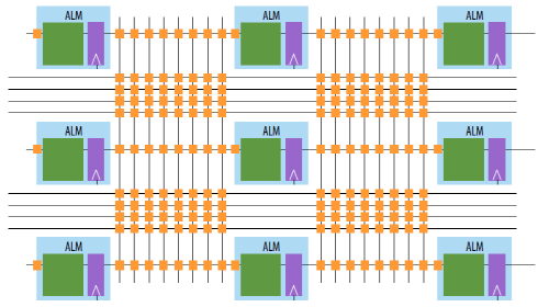
Figure 3 shows a small part of the FPGA fabric, consisting of 9 ALMs and interconnect wiring connecting them. The location of the hyper-register is indicated by a square at the intersection of each horizontal and vertical wiring section.
[Figure 3] HyperFlex architecture with "omnipresent register" design
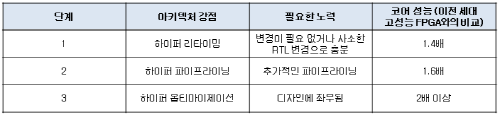
To maximize design performance using the HyperFlex architecture, developers utilize a three-step process of register retiming, pipelining, and design optimization based on familiar design techniques. Hyper-Registers enable developers to dramatically improve design performance compared to what was possible with existing FPGA architectures by utilizing familiar design techniques. When these general techniques are implemented using Hyper-Registers instead of registers within the ALM, their names change to Hyper-Retiming, Hyper-Pipelining, and Hyper-Optimization. Table 1 summarizes the performance improvements achieved at each stage.
[Table 1] 3-Step Process to Maximize Performance Using HyperFlex Architecture
As process geometry shrinks, interconnect latency between ALMs exerts a dominant influence, limiting performance. One of the key aspects of the HyperFlex architecture is placing HyperResistors in the interconnect wiring section, where this problem can be best addressed.
Hyper Retiming
Design retiming is achieved using HyperResistors located in the interconnect wiring. This process requires little to no user effort while delivering an average performance improvement of 1.4x compared to previous generation high-performance FPGAs for Stratix 10 devices. HyperRetiming eliminates critical paths by moving registers from the ALM to the interconnect, balancing latency between registers, and enabling the design to execute at faster clock frequencies. Since HyperResistors exist throughout the interconnect, register locations are distributed at a fine level. Conventional retiming requires additional FPGA logic and wiring resources, and necessitates recompiling, refitting, and rewiring the design. In contrast, hyper-retiming does not use additional FPGA resources and is performed after placement and wiring operations, so core performance can be significantly improved with little to no effort from the developer.
Pipelining and retiming of the design are performed using HyperRegister. This technique requires minimal user effort while delivering an average performance improvement of 1.6 times compared to previous generation high-performance FPGAs for Stratix 10 devices. Hyperpipelining eliminates long wiring delays by adding extra pipeline stages to the interconnects between ALMs, allowing the design to run at faster clock frequencies.
This also allows for fine-grained selection of register locations thanks to the hyper registers situated throughout the interconnect. Like hyper retiming, hyper pipelining does not use additional FPGA logic and wiring resources and is performed after placement and wiring operations.
Hyper-optimization
Some designs accelerate data paths with hyper-retiming and hyper-pipelining, but are then constrained by control logic such as long feedback loops and state machines. To achieve higher performance, the structure of these logic parts must be reformed to utilize functionally equivalent feed-forward or pre-compute paths instead of long combinatorial feedback paths. While this method may require more effort depending on the design, it delivers more than double the performance improvement compared to previous generation high-performance FPGAs in the case of Stratix 10 devices. In conventional architectures, this process is called design optimization. However, in the HyperFlex architecture, this process is called hyper-optimization because the benefits of hyper-retiming and hyper-pipelining are applied to feed-forward or pre-compute paths due to hyper-registers.
Hyper-Aware Design Flow
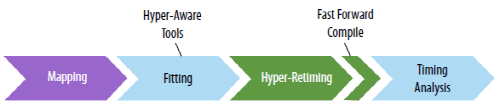
Altera has developed a powerful series of new tools and integrated them into Quartus II design software, which help system developers maximize their design productivity by fully utilizing the HyperFlex architecture. Figure 4 shows the design flow of Quartus II Hyper-Aware.
[Figure 4] Hyper-Aware Design Flow
Fast Forward Compile
This new tool guides users through the performance optimization process by identifying performance-limiting areas in the design, determining where and how many pipelines can be used for performance improvement, and highlighting bottlenecks (such as long feedback loops) on critical control paths. The tool also enables developers to optimally utilize the new HyperFlex architecture by predicting the performance of their existing designs when implemented on Stratix 10 devices.
Hyper Retimer
The Hyper Retimer phase takes place towards the end of the design compilation process. This phase optimizes performance through optimal fine-grained Hyper Retiming using Hyper Registers after placement and wiring operations. This phase also allows users to implement Hyper Pipelining much more easily than conventional pipelining. The Fast Forward Compile Report feature identifies which clock domains can benefit from pipeline stages and how many are required. Once the developer modifies the RTL and places a predetermined number of pipeline stages at the boundaries of each clock domain, HyperRetimer maximizes performance by automatically placing registers in optimal positions within the clock domains. Thanks to this automatic placement feature and the Fast Forward Compile Report, pipelining becomes easier than ever before.
Hyper-Aware Algorithm
The Hyper-Aware algorithm used during synthesis, placement, and wiring operations enables the tool to save logic resources by predicting which registers can be moved from the ALM to the Hyper-Registers within the interconnect wiring.
conclusion
The combination of the new HyperFlex architecture and Intel's 14nm Tri-Gate process technology enables Stratix 10 FPGAs and SoCs to achieve previously unimaginable levels of performance, integration, and power efficiency in programmable logic devices. The features provided by the Stratix 10 device are as follows:
- Doubled core performance and more than 5 times higher integration density compared to the previous generation Stratix V FPGA
- Up to 70 percent less power consumption than Stratix V FPGAs at the same performance
- Logic capable of operating at 1 GHz, built-in memory, and DSP blocks
- Built-in quad-core 64-bit ARM Cortex-A53 hard processor system (SoC version)
- Hyper-Aware Design Flow
- Familiar FPGA design techniques supported by proven Quartus II software
[References]
1. Global Internet Capacity Reaches 77 Tbps despite Slowdown
www.telegeography.com/press/press-releases/2012/09/06/global-internetcapacity-
reaches-77-tbps-despite-slowdown/index.html
2. Gartner Says the Internet of Things Installed Base Will Grow to 26 Billion Units by
2020
www.gartner.com/newsroom/id/2636073
3. 400 Gbps Ethernet Study Group
www.ieee802.org/3/400GSG/
4. Cisco Visual Networking Index: Forecast and Methodology, 2012-2017
www.cisco.com/c/en/us/solutions/collateral/service-provider/ip-ngn-ip-nextgeneration-
network/white_paper_c11-481360.html
5. Satellite Backhaul & Trunking Are Capacity Driven Markets
www.nsr.com/news-resources/the-bottom-line/satellite-backhaul-trunking-arecapacity-
driven-markets/
6. Cisco Visual Networking Index (VNI) Global Mobile Data Traffic Forecast Update
www.ciscoknowledgenetwork.com/files/222_03-27-2012-CKN_Cisco_Mobile-
VNI-Forecast_2012_CKN_Deck.pdf
7. Global Census Shows Datacentre Power Demand Grew 63% in 2012
www.computerweekly.com/news/2240164589/Datacentre-power-demand-grew-
63-in-2012-Global-datacentre-census
8. My New Study of Data Center Electricity
www.koomey.com/post/8323374335


.png)

 Published2015.07.07 19:17