


Samsung Electronics Breaks Technological Limitations, Ushering in the '10nm-Class DRAM Era'
 Published2016.04.05 17:23
Samsung Electronics has broken through the limits of semiconductor technology and ushered in the world's first '10-nanometer class DRAM era'.
Samsung Electronics announced that it has been mass-producing the world's smallest 10-nanometer (1 nanometer: 1 billionth of a meter) 8Gb (gigabit) DDR4 (Double Data Rate 4) DRAM since February.
Following the world's first mass production of 20-nanometer 4Gb DDR3 DRAM in 2014, Samsung Electronics has once again broken through the limits of semiconductor microfabrication with the mass production of 10-nanometer 8Gb DDR4 DRAM, setting a new milestone in memory technology.
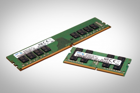
This product incorporates three innovative technologies: 'ultra-high integration design technology,' 'Quadruple Patterning Technique,' and 'ultra-uniform dielectric film formation technology.' Accordingly, it has further enhanced the manufacturing competitiveness of premium products by mass-producing 10-nanometer class DRAM without introducing next-generation extreme ultraviolet (EUV) lithography equipment.
'Ultra-high integration design technology' is a next-generation semiconductor design technology independently developed by Samsung Electronics, which has increased productivity by more than 30% compared to 20nm 8Gb DDR4 DRAM.
Application of three innovative technologies, including quadruple photolithography technology
Achieved 3,200Mbps, over 30% faster operating speed compared to existing 20nm.
In addition, the 10-nanometer (1x) 8Gb DDR4 DRAM applies ultra-high-speed and ultra-low-power design technology, enabling an operating speed of 3,200Mbps, which is more than 30% faster than the existing 20-nanometer DRAM, and can reduce power consumption by 10% to 20% depending on the operating state, providing an optimal solution for the next-generation enterprise server market.
Samsung Electronics has opened a new horizon in core DRAM process technology by being the first in the industry to implement 'Quadruple Photolithography,' which was previously applied to NAND flash mass production to overcome the limitations of microfabrication. Unlike NAND flash, where a cell (the smallest unit of information storage) consists of a single transistor, DRAM cells are composed of a stacked structure of transistors and capacitors.
For this reason, the development difficulty of 10-nanometer 8Gb DRAM was high due to miniaturization, as it required creating more than 8 billion perfectly functioning cells by arranging high-capacity capacitors at nanometer intervals on top of ultra-high-speed transistors.
Samsung Electronics overcame these DRAM process limitations through 'quadruple photolithography technology'By overcoming this, we have secured the foundational technology to mass-produce next-generation 10-nanometer class (1y) DRAM in a timely manner. In addition, DRAM requires 'ultra-uniform atomic dielectric film formation technology' to store a sufficient amount of charge in ultra-fine capacitors.
Following the PC and server markets, we continue to dominate the ultra-high-resolution smartphone market.
10-nanometer class DRAM secures excellent cell characteristics that enable stable operation even at higher speeds by uniformly forming the dielectric film of the capacitor with ultra-thin atomic materials in the angstrom (one-tenth of a nanometer) range. Samsung Electronics plans to mass-produce 10-nanometer class mobile DRAM this year that simultaneously increases capacity and performance, with a strategy to continue dominating the ultra-high-resolution smartphone market following the PC and server markets.
Jeon Young-hyun, President of Samsung Electronics’ Memory Business, stated, “10nm-class DRAM will provide global IT customers with the most efficient system investment solutions,” adding, “Through the future launch of next-generation ultra-high-capacity, ultra-low-power mobile DRAM, we will contribute to enabling leading companies in the mobile market to release more innovative products in a timely manner, thereby significantly enhancing user convenience for global consumers.”
Going forward, Samsung Electronics plans to build a full lineup ranging from 4GB (gigabyte) DDR4 modules for PCs to 128GB modules for enterprise servers, and to drive the growth of the premium DRAM market by continuously expanding the proportion of 10nm-class production to meet the high demand for ultra-high-capacity mobile DRAM.
Comments
Related news
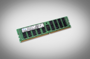
Mass production of 128-gigabyte server DRAM modules using 3D TSV stacking technology
Samsung Electronics has begun mass production of the world's first '128-gigabyte (GB) server-use (RDIMM) DRAM module' that simultaneously achieves maximum capacity and ultra-low power consumption by applying three-dimensional TSV stacking technology.
2015.11.26by 명세환 기자
Samsung Electronics to Mass-Produce 256GB UFS Internal Memory for Smartphones
Samsung Electronics will begin mass producing the industry's first 256-gigabyte UFS (Universal Flash Storage) embedded memory for next-generation smartphones starting this month. The 256GB UFS is nine times faster than high-performance microSD cards (based on sequential read speed) and nearly twice as fast as entry-level SSDs for notebooks, and is expected to elevate the memory storage market's growth paradigm from capacity-centric to performance-centric.
2016.02.25by
Can Samsung's IoT platform, 'ARTIK,' succeed?
Samsung Electronics' ARTIK is a ultra-compact IoT module composed of a processor (AP), memory, communication, and sensor. As evidenced by the company's emphasis that it is a platform with software/drivers, storage, security solutions, development boards, and cloud functionality integrated into a single module, Samsung expressed confidence that developers can quickly and easily commercialize IoT devices utilizing ARTIK.
2016.03.07by 신윤오 기자

Intel Unveils Next-Generation 'Core Ultra Series 3' and vPro Platform for Enterprise PCs
Intel has officially unveiled the "Intel Core Ultra Series 3" for next-generation enterprise PCs and the latest vPro platform, addressing a wide range of demands from enterprise notebooks to high-performance workstations.
2026.03.26by 배종인 기자

ROHM Launches ESD Protection Diode Compatible with High-Speed Interfaces of 10Gbps or Higher
Semiconductor specialist ROHM has developed the 'RESDxVx series' of ESD (electrostatic discharge) protection diodes capable of responding to next-generation high-speed data communication environments exceeding 10Gbps, simultaneously enhancing both signal quality maintenance required in high-speed interfaces and IC protection performance.
2026.03.26by 배종인 기자











