


PCB Market and Technology Trends (Part 2) Embedded PCBs are being adopted in large numbers, and automotive high-power boards are on the rise
 Published2016.04.25 19:49
Build-up substrate circuit width 35μm, CSP to be maintained at 12μm/12μm until 2018
As mobile devices become more high-performance, embedded circuit boards are expected to be adopted in large numbers this year, and as HEV/EV vehicles increase, the use of high-power circuit boards is expected to increase.
According to the Electronic Circuit Board Industry Status (2016) report published by the Korea Electronics Circuit Industry Association, the roadmap for PCB (printed circuit board) technology shows that while build-up boards currently being mass-produced will continue to grow in order to achieve lightweight, slim design and fine pitch implementation, flexible boards are expected to show somewhat slower growth.
In addition, according to the report, the IC substrate (IC-Substrate) is expected to maintain the 25/25μm level for PBGA and the 12μm/12μm level for CSP until 2018, and the demand for metal substrates will continue to grow in special specification fields.
Contrasting growth of rigid and flexible substrates
Build-up substrates are widely used in all electronic products and are continuously growing. .
The build-up substrates used in the main boards of mobile devices have 8 to 12 layers and have a 1+N+1 (1 Build) to 4+N+4 (4 Build) structure, and the form is changing from 'staggered via' to 'Staked via', and the adoption of the All layer Build-up (Full Stacked via) structure is increasing.
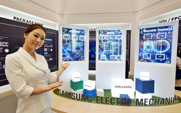
▲ Samsung Electro-Mechanics participated in the KPCA Show last year and showcased its cutting-edge PCB technology for smartphones, notebook PCs, and wearables.
Embedded substrates are being actively used in some cases by utilizing materials for embedded passives and chip embedding, which mounts chips inside the substrate. Optical substrates are being developed in various forms by academia, industry, and research to solve problems such as high capacity, high-speed transmission, and noise.
The technology level of the build-up substrate is changing toward becoming narrower, smaller, and thinner, with a circuit width of 35 μm, hole diameter of 150 μm, micro via diameter of 75 μm, ball pitch of 350 μm, and product thickness of 0.50 mm for 10 layers.
In 2015, the market for flexible printed circuit boards expanded from the previous use in mobile phone hinges, small cameras, liquid crystal displays, and keypads to the use of up to 20 FPCs in smartphones. Although it grew rapidly, demand has continued to show a somewhat gradual growth trend since 2014 as the number of low- to mid-priced products has increased.
In the case of Rigid-Flex boards for mobile phones, build-up technology was applied to most products, and in the case of multilayer flexible boards, build-up technology was applied to most products. The build-up technology applied to Rigid-Flex boards is usually a 1+4+1 or 2+2+2 structure, which is a technology with 2 builds or less.
The circuit width of multilayer flexible substrates is expected to decrease from 50 μm in 2014 to 45 μm in 2016, and then to 30 μm in 2018. The hole diameter is expected to decrease from 100 μm in 2014 to 75 μm in 2016, and the micro via diameter is expected to decrease from 100 μm in 2014 to 75 μm in 2016 and to 50 μm in 2018. In the case of embedded flexible substrates, there is a difficulty due to the thickness issue, and although a flexible substrate for embedded passives has been developed by Rigid-Flex, it has been found that there are no plans for adoption as of now.
IC substrate (IC-Substrate) reflecting high-difficulty technology
PBGA (Plastic Ball Grid Array) currently has an I/O pin count of 200 to 900, and Line/Space is at the 25/25μm level in 2016 and is expected to remain unchanged until 2018. In addition, the market share continues to decline due to flip chips, and it is expected to show an annual growth rate of less than 2%.
CSP(Chip Scale Package) is the most basic technology for realizing high-density circuits, and the most basic technology is microcircuit formation and thin build-up technology, and the core technology is Blind/Buried Via processing and stacking lamination technology that can obtain freedom of other layers. In 2014, Line/Space was at 15μm/15μm and it is expected to be maintained at 12μm/12μm until 2018.
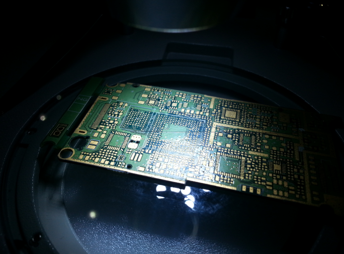
▲ PCB introduced at the exhibition hall.
As of 2015, FC-BGA is trending with Line/Space of 15μm/15μm, and especially for high-performance logic devices, mass production is underway with 8μm/10μm, Via dia of 50μm, and Bump Pitch of 130μm. As the 2016 pattern requires high-difficulty technology with 8μm/10μm and a bump pitch of 120μm, it is expected that FC-BGA products requiring existing SOP (Solder on Pad) bumping will be replaced by micro ball mounting technology or copper bump technology using plating.
As of 2104, FC_CSP is mass-produced with a 2-2-2 build-up structure with a 4- to 6-layer structure and a build-up layer Line/Space of 15/15. In addition, it is analyzed that in 2016, high-difficulty technologies such as a 4- to 8-layer structure, a 12μm/12μm pattern, a 60μm ultra-small via, and a 120μm bump pitch will be required.
“With the recent trend of narrow bezels, ultra-slim and flexible mobile devices,
COF adoption demand (currently COG) is increasing and mobile
“As resolution increases, pattern counts are likely to increase dramatically.”
As of 2014, BOC (Board on Chip) is being mass-produced with a minimum thickness of 1~2 layers of 130μm and a Line/Space of 25/25μm. In addition, in 2016, it is analyzed that the minimum thickness of 1~3L will be 120μm, the pattern will be 25μm/25μm, the CNC drill and pad size will be 60μm/150μm, and the SR ink thickness will be 15μm.
As of 2014, SIP (System In Package) is being mass-produced with a minimum thickness of 180μm for 4 to 8 layers and a Line/Space of 20μm/20μm. Also, in 2016, the minimum thickness of 4 to 8 layers will be 150 μm, the pattern will be 15 μm/15 μm, the CNC drill and pad size will be 60 μm/130 μm, and the SR ink thickness will be 15 μm.
The lead thickness of COF (Chip on Film) is expected to be maintained at 8μm until 2016, and the pattern pitch is scheduled to start mass production from 22 pitch in 2014 to 20 pitch in 2016. However, 25-pitch products are expected to be mass-produced primarily for important display applications due to increased quality costs for pattern miniaturization. Recently, demand for COF adoption (currently COG) is increasing due to the narrow bezel, ultra-slim, and flexible display of mobile devices, and the pattern count is likely to increase rapidly as the resolution of mobile devices increases.
Expansion of embedded boards due to high performance of smartphones and tablet PCs
Application of optical substrate for high-speed, large-capacity signal processing between display panel and set-top box
Since 2015, there has been an increase in the number of cases where active components are embedded in electronic packaging companies rather than embedded in embedded boards, and there is an increasing demand for cost-effective embedded boards. In 2015, it is expected that embedded technology will be widely applied and activated in the form of embedded passive components modules, starting with the embedding of ICs with relatively few pins and simple design, and gradually expanding to the Embedding Die Substrate of PMIC and RFIC.
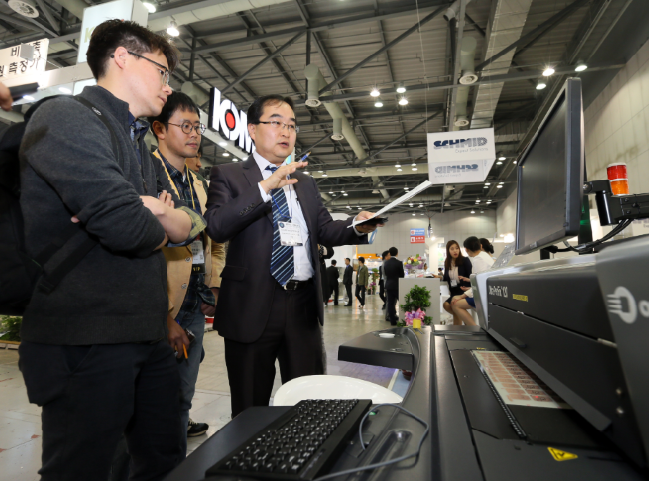
▲ Attendees at last year’s KPCA Show listen to an explanation of PCB products. (KPCA Show website)
Since 2015, embedded circuit boards have been adopted for many packages and module parts inside smartphones and tablet PCs due to their high performance, and it is expected that embedded circuit boards will be adopted in large numbers starting in 2016 due to this trend.
Even in 2016, the optical substrate was not technologically mature, and was applied to some communication and computer backplanes. In the future, with the trend toward larger, more flexible, and more transparent displays, the optical substrate is expected to be applied to high-speed, large-capacity signal processing between display panels and set-top boxes.
Application to cell phones/mobile devices seems difficult for the time being. Waveguides for optical substrates require high transmittance and high heat resistance, and Dow Corning is currently producing a small quantity of materials that satisfy both requirements for R&D purposes.
Metal substrate, other than the TV market, the lighting market is the largest market
Increasing use of high-power substrates for inverters/converters due to increase in HEV/EV vehicles
Rigid LED substrates occupy about 80% of the domestic market, and most of them are produced in single-sided/double-sided product forms. Rather than the trend toward smaller hole diameters, the design and production of products are being applied in the direction of eliminating pores.
Metal PCBs, which used to replace the backlight of LCD TVs, are judged to have already lost their market dominance due to changes in specifications, and the lighting market is a large market aside from the TV market. The increase in the use of metal PCBs is slowing down due to market price pressure caused by the reduction in lighting prices, but demand is expected to continue in special specifications such as security lights.
Global automobile shipments in 2014 were 87 million units, similar to the previous year, and grew 0.5% in 2015 to 88 million units. While growth of conventional vehicles is expected to average about 2.1% through 2016, growth of EV/HV/PHV/FCV is expected to grow by about 18.8% in 2016, including 6.8% in 2015.
The main use of the circuit board for the entire field was in the past ECU/telematics/ABS/TCU, and the main specifications were multilayer circuit boards with 4 to 8 layers and double-sided circuit boards, but as we enter the era of HEV/EV automobiles, the use of high-power Heavy Cu circuit boards is increasing due to the increased use of inverters/converters that supply electricity to electric motors.
Heavy Cu substrates generally refer to products with a Cu thickness of 3Oz (105μm) or more, but due to various issues such as substrate circuit implementation capabilities, the market is currently dominated by substrate product groups centered on 2Oz (70μm), but it is expected that product groups centered on 4Oz or more will expand in the future for the purpose of high current transmission and strengthening substrate durability.
Comments
Related news

Achieve Complete Verification with the Stronger Mentor PCB Design Validation Tool 'HyperLynx'
Mentor Graphics Korea (CEO Yang Young-in) announced the launch of a new version of its PCB design validation solution 'HyperLynx®'. The latest version of 'HyperLynx®' enables integrated verification of signal and power integrity, 3D electromagnetic solving, and high-speed design rule checking all at once. Based on the widely-used HyperLynx signal integrity/power integrity (SI/PI) application, this product provides a comprehensive set of analysis technologies that enable designers to design any type of high-speed digital PCB, according to the company.
2016.04.04by
PCB Market and Technology Trends (Part 1) High-function mobile and battlefield boards drive growth in domestic PCB market
The global PCB (printed circuit board) market is expected to grow at an average annual rate of 3.1% through 2019, and the domestic PCB market is also anticipated to return to growth this year following a decline in the previous year. According to the Electronic Circuit Board Industry Status Report published by the Korea Electronics Circuit Industry Association, high-end substrates for mobile and network applications, as well as automotive electrical system substrates, are expected to lead the upward trend in the PCB market this year.
2016.04.18by 신윤오 기자

Intel Unveils Next-Generation 'Core Ultra Series 3' and vPro Platform for Enterprise PCs
Intel has officially unveiled the "Intel Core Ultra Series 3" for next-generation enterprise PCs and the latest vPro platform, addressing a wide range of demands from enterprise notebooks to high-performance workstations.
2026.03.26by 배종인 기자

ROHM Launches ESD Protection Diode Compatible with High-Speed Interfaces of 10Gbps or Higher
Semiconductor specialist ROHM has developed the 'RESDxVx series' of ESD (electrostatic discharge) protection diodes capable of responding to next-generation high-speed data communication environments exceeding 10Gbps, simultaneously enhancing both signal quality maintenance required in high-speed interfaces and IC protection performance.
2026.03.26by 배종인 기자

ST Launches 75V Drive IC Targeting 48V Industrial Motor Driving
ST Microelectronics has unveiled the 'STSPIN9P' series of 75V motor drive ICs tailored for 48V-class industrial drive system design. The new product family is characterized by half-bridge and full-bridge configurations that enable design scalability according to motor type and output conditions. Power supply circuits, protection functions, and current sensing circuits are integrated on-chip to simplify system configuration, and the devices are designed to support applications up to 500W maximum. The company plans to provide reference designs and demo boards to support development and evaluation in industrial automation, robotics, pumps, fans, lighting, and textile machinery.
2026.03.26by 배종인 기자











