



[Reporter's Notebook] Forget Moore's Law, It's Semiconductor Packaging Now
 Published2016.08.23 10:15
“Semiconductor scaling is dying, but packaging will live on”
At the recent JEDEC Mobile & IoT Forum, Huawei's Dr. Wei Koh concluded his presentation by exclaiming, "As the shrinking technology of semiconductor CMOS chips reaches its limit, packaging technology, a post-process of semiconductors, is becoming an alternative for system integration."
Yes. The so-called 'Moore's Law', which states that 'the integration of microchips doubles every 18 months', is now in an era where integration beyond Moore's Law, or 'More than Moore' (MtM), is needed.
The reason we say that a new era has arrived, as you all know, has to do with the advent of new smart devices. This is because the role of highly integrated system semiconductors is expanding from high-performance smartphones, tablet PCs, and wearable devices to smart TVs, automobiles, robots, and bio fields.
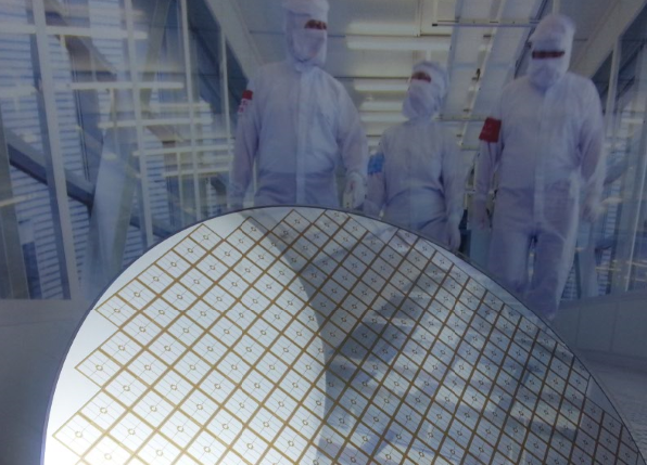
▲ Infineon's eWLB package, called the 'mother of fan-out WLP technology', can reduce the size by about 30% compared to the lead frame package.
This is why Dr. Wayco called packaging a “white knight” running to save wafers. With the resurrected cutting-edge PSI (Packaging System Integration) technology, various technologies such as PoP (Package on Package), FOWLP (Fan-out Wafer Level Package), SiP (System in Packages), and Embedded Solutions are competing.
To realize integrated package technology, advanced IC technologies such as fine pitch interconnect, more I/O, multi-chip stacking, multi-chip package, 3D stacking, and 3D WLP are required, and wafer level processing called 'mid-end' is required. Modular applications such as security ID modules, camera modules (CIS), MEMS sensors, health sensors, RF modules, and PM modules are also required for mobile and IoT.
Based on this, various technologies are being developed in packaging technology for greater integration, such as die-level integration (C2C, 3D stack), wafer-level integration (Fan-in, Fan-out), substrate-level integration (chip and passive components embedded), board-level integration (embedded IC, embedded MCP, embedded SiP, embedded multi-die interconnect bridge), and system-level integration.
As such, the packaging market has the potential to grow by more than 30% annually to over $30 billion by 2020, and semiconductor companies are fiercely competing to secure packaging technology. In particular, as mentioned above, in the post-PC era, wearables and fitness devices are expected to form a huge market (41% growth rate) to replace stagnant smartphones and tablets, so the importance of packaging technology is increasing.
For example, Samsung S7 integrates Qualcomm Snapdragon 820 SoC and SK Hynix LPDDR4 memory (3733Mbps) using PoP, and Apple A8/A9 also uses PoP with a pitch of only 0.35mm. AMKOR is applying the second-generation PoP, TMV (Through Mold Via), which enables high density and reduced height along with changes in the memory structure. TMV technology provides a thin substrate and stable packaging in devices with a large die-to-package ratio.
Recently, semiconductor companies have shown great interest in packaging technologies, especially FOWLP (Fan Out Wafer Level Package) technology. This is because SiP, which mounts chips with various functions in a single package, is very advantageous in the mobile device and IoT markets where quick market launch is key.
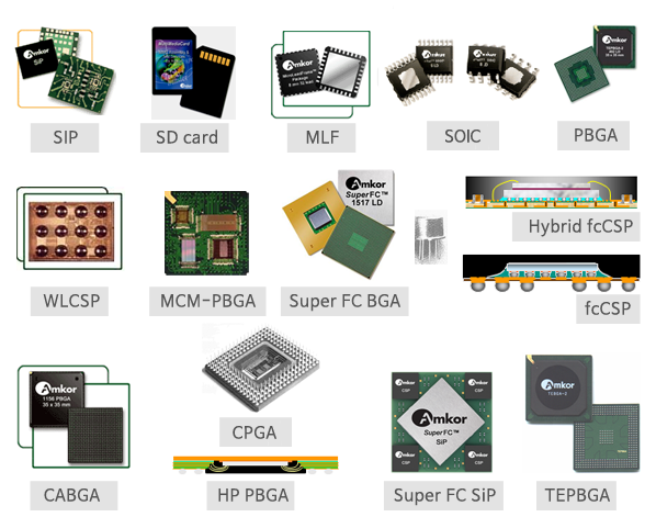
▲ Various types of semiconductor packages (Source: Amkor Korea)
Since general WLP requires that all package I/O terminals be placed inside the chip, the ball size and pitch must be reduced as the chip size decreases, so the standard ball layout cannot be used. For this reason, FOWLP (package I/O terminal placement outside the chip), which can use the standard ball layout as it is even if the chip size decreases, is attracting attention. In particular, FOWLP has a simple packaging process and can be implemented with a thin thickness, so it can be miniaturized and thinned more than BGA, and it has excellent thermal and electrical characteristics, making it suitable for mobile products.
Infineon's eWLB is the most representative one, but many companies are researching various fan-out techniques, including Amkor's SLIM and SWIFT technologies and TSMC's InFO and Deca M series. In particular, Infineon's eWLB package, called the 'mother of fan-out WLP technology', can reduce the size by about 30% compared to the lead frame package.
The semiconductor industry has already entered a new packaging paradigm era. Even though FOWLP packaging technology is in the spotlight, there are still many difficulties to overcome, such as electromigration, thermal issues, EDA tools, and warpage issues. To this end, standardization, design, materials, and process improvements must also continue to develop.
No less than Moore's Law, the 'Law of Packaging' is preparing for a new semiconductor era.
Comments
Related news
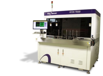
KLA-Tencor Launches New Product for Advanced Semiconductor Packaging
2015.05.18by 명세환 기자

Intel Unveils Next-Generation 'Core Ultra Series 3' and vPro Platform for Enterprise PCs
Intel has officially unveiled the "Intel Core Ultra Series 3" for next-generation enterprise PCs and the latest vPro platform, addressing a wide range of demands from enterprise notebooks to high-performance workstations.
2026.03.26by 배종인 기자

ROHM Launches ESD Protection Diode Compatible with High-Speed Interfaces of 10Gbps or Higher
Semiconductor specialist ROHM has developed the 'RESDxVx series' of ESD (electrostatic discharge) protection diodes capable of responding to next-generation high-speed data communication environments exceeding 10Gbps, simultaneously enhancing both signal quality maintenance required in high-speed interfaces and IC protection performance.
2026.03.26by 배종인 기자

ST Launches 75V Drive IC Targeting 48V Industrial Motor Driving
ST Microelectronics has unveiled the 'STSPIN9P' series of 75V motor drive ICs tailored for 48V-class industrial drive system design. The new product family is characterized by half-bridge and full-bridge configurations that enable design scalability according to motor type and output conditions. Power supply circuits, protection functions, and current sensing circuits are integrated on-chip to simplify system configuration, and the devices are designed to support applications up to 500W maximum. The company plans to provide reference designs and demo boards to support development and evaluation in industrial automation, robotics, pumps, fans, lighting, and textile machinery.
2026.03.26by 배종인 기자











