



Samsung Electronics Mass-produces Longer-lasting Wearable APs Using '14nm FinFET'
 Published2016.10.12 16:59
Implementing optimized ultra-compact solutions with state-of-the-art packaging technology
Samsung Electronics announced the mass production of the 'Exynos 7270,' a wearable-dedicated AP based on the 14nm FinFET process.
Following the expansion of the application of its high-performance, low-power 14nm advanced process—previously used in premium mobile APs—to entry-level models earlier this year, Samsung Electronics has now, for the first time in the industry,
It was also applied to APs dedicated to wearables.
The 'Exynos 7270', which uses a dual core (Cortex-A53), utilizes a 14nm process, improving operating power efficiency by more than 20% compared to existing 28nm-based products, enabling wearable device users to use the device for a long time on a single charge.
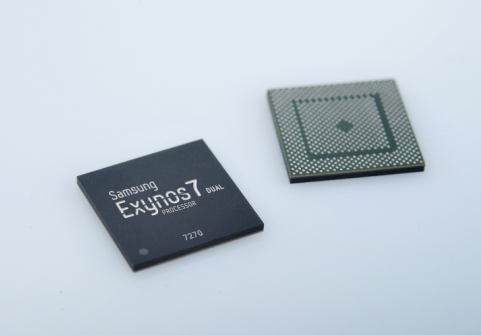
In addition, by integrating various connectivity functions such as Cat.4 LTE modem, Wi-Fi, Bluetooth, FM radio, and Global Navigation Satellite System (GNSS) into a single chip, it provides wearable device manufacturers with upgraded functionality and design convenience, including the ability to use communication network-based convenience features independently.
In addition, by minimizing system area through state-of-the-art packaging technology, it provides low-power, ultra-compact products optimized for wearable devices.
Integrated AP, DRAM, NAND Flash, and PMIC into a single package
By applying advanced packaging technology (SiP-ePoP) that incorporates AP, DRAM, NAND flash, and even PMIC into a single package, it not only implemented more functions within the same 100mm² area as the previous generation product but also reduced the package height by approximately 30%.
In addition, it provided wearable device manufacturers with a reference development platform consisting of APs, displays, NFC, and various sensors, enabling customers to develop products more quickly and conveniently.
"This product presents a new paradigm for wearable-dedicated SOCs based on low-power processes, modem and connectivity integration, and innovative packaging technology," said Heo Kuk, Senior Vice President of Strategy Marketing Team at Samsung Electronics System LSI Business Division. "It will make a significant contribution to the popularization of wearables by enabling significantly longer device usage time and a slim design."
Comments
Related news

AMD Unveils 14nm FinFET Process-Based GPU Architecture
AMD unveiled a new Polaris GPU architecture at CES 2016. The company stated that this new architecture, based on significantly improved design, delivers high performance per watt and incorporates the latest features such as HDR monitor support. AMD anticipates that it will be able to ship GPU products based on the Polaris architecture starting from mid-2016.
2016.01.05by
Samsung Electronics applies 14nm FinFET process to achieve both performance and power efficiency
Samsung Electronics has unveiled a new budget-tier mobile SoC called "Exynos 7870," which delivers excellent performance and power efficiency based on advanced 14-nanometer FinFET process technology. Samsung Electronics' newly launched single-chip solution, the Exynos 7870, is the first budget-tier SoC to incorporate 14-nanometer process technology. This move represents Samsung Electronics' strategic expansion of the 14-nanometer process—previously applied only to premium products—to budget-tier SoC products, thereby strengthening its SoC business.
2016.02.17by
Targeting the IoT market as well, Samsung begins mass production of Exynos APs with integrated connectivity.
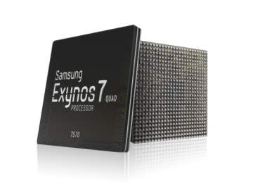
Samsung Electronics has announced that it has begun mass production of the "Exynos 7570," a cost-effective mobile AP that integrates modem and connectivity functions based on the industry's first high-performance, low-power 14-nanometer FinFET process. Samsung Electronics solidified its advanced process technology leadership by beginning mass production of a premium mobile AP based on the 14-nanometer process last year, and by applying 14-nanometer process technology to budget-tier products earlier this year. With the mass production launch of the new cost-effective product "Exynos 7570," Samsung Electronics has further expanded its lineup of 14-nanometer-based budget-tier mobile APs and created an opportunity to provide high-performance/low-power solutions not only to various smartphones but also to IoT products. The "Exynos 7570" is a quad-core product with 70% improved CPU performance and over 30% improved power efficiency compared to the previous generation 28-nanometer product.
2016.08.30by 김수지 기자

ESP32 Development Environment Selection and GPS Application Implementation
The ESP32 is a microcontroller that integrates Wi-Fi, Bluetooth, 12-bit ADC, capacitive touch, PWM, DAC, and UART in a single SoC. However, the abundance of features does not by itself solve the designer's problems. The real challenges lie in selecting the appropriate development environment, determining which pins can be used and which must be avoided, and converting raw data from modules into usable information. This document addresses ESP32 peripheral constraints (ADC2 and Wi-Fi coexistence limitation, UART1 occupancy, ADC non-linear regions), the trade-offs between Arduino IDE and ESP-IDF, and the process from connecting NEO-6M/NEO-M8N GPS modules to UART2, parsing NMEA sentences, and visualizing routes in Google Earth, all organized based on documented references.
2026.10.12by 편집부

MIPI CSI-2, DSI-2, C-PHY, D-PHY Test Solution Technical White Paper
The MIPI interface adopts a burst mode that transitions between low-power (LP) and high-speed (HS) states for low-power consumption, and in return, strict timing rules are imposed on state transitions. Additionally, the high-speed section operates as a packet-based protocol with headers, ECC, and CRC, so verification engineers must handle waveforms and protocols simultaneously. Traditional configurations combining general-purpose oscilloscopes and AWGs reveal limitations in setup complexity, measurement uncertainty, and lack of reproducibility when faced with these requirements. This white paper, based on webinar materials, organizes the structure of this problem and describes how the SV5C-DPTXCPTX generator for receiver testing and SV5C-DPRXCPRX analyzer for transmitter testing integrate state transition testing, stressed eye testing, and protocol analysis into a single bench, along with their application boundaries.
2026.10.12by 편집부











