



The dilemma of the Chinese semiconductor industry, heated by 3D NAND and foundry investments, is
 Published2017.02.13 17:45
With the semiconductor market expected to continue its growth this year, driven by investments in 3D NAND and foundry services, what are the concerns of China, which accounts for one-third of the global semiconductor equipment investment market?
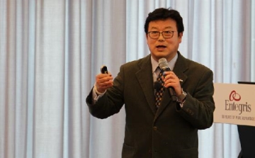
Clark Tseng, an analyst at SEMI (Semiconductor Equipment and Materials International), who participated in a press conference held ahead of SEMICON 2017, which took place from the 8th to the 10th of last week, stated, "Money is not the issue; the obstacles are the problem of recruiting competent professional engineers from Taiwan and Korea and regulatory issues regarding the acquisition of overseas companies."
In a presentation on the outlook for Chinese fab investments, analyst Clark Chang stated, “China will make significant investments in foundry and 3D NAND from this year through next year, leading to a 2–3% growth in production capacity,” adding, “As new fab projects in China continue to increase, there are concerns that foundry capacity may become oversupplied.” "In particular, if Chinese memory fabs begin full-scale operation after 2020, an oversupply could occur in memory as well," they predicted.
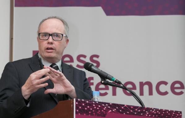
SEMI analyst Dan Tracy said that fab investment will increase due to 3D NAND, advanced foundries, and increased investment in China, and in particular, 200mm fab investment will increase.
Earlier, SEMI Senior Analyst Dan Tracy stated, “Despite the existence of economic uncertainty as in recent years, the semiconductor market is expected to have a positive future through 2020, driven by technological advancements and government support policies,” adding, “Fab investment will increase due to 3D NAND, advanced foundries, and expanded investment in China, and 200mm fab investment in particular will rise.”
We took a detailed look at the semiconductor market as revealed by these SEMI analysts.
SEMI viewed the overall semiconductor market positively, although it expressed concern about some oversupply due to the current aggressive expansion of investment. Earlier regarding the semiconductor industry this year, Gartner predicted the highest growth rate at 7.2%, while institutions such as VLSI (6.0%), IC Insights (5.0%), IBS (4.6%), Crowan LRA (4.4%), and WSTS (3.3%) rushed to release positive forecasts.
These organizations identified storage, industrial, wireless, and automotive sectors as key markets, and listed big data infrastructure, 5G infrastructure, 5G devices, image processing, IoT, ADAS, and storage systems as high-growth areas by 2020. In particular, the automotive industry selected connected cars, autonomous vehicles, and electric vehicles with powertrains as key trends. Gartner predicted that 80% of cars will be equipped with connected features by 2020.
Samsung, Intel, and others race to expand fabs in China
Increased 3D NAND fab investment drives equipment investment
Senior Manager Dan Tracy noted that investments in 3D NAND and advanced foundries increased until last year and predicted that these sectors would continue to drive investment this year. Regarding NAND, Micron expanded its fab in Singapore, and the Toshiba/Flash Alliance established a new R&D center along with fab expansion. Intel and Samsung also expanded their fabs in China, while SK Hynix and XMC expanded and established new 3D NAND fabs, respectively.
Looking at the companies investing in fab equipment (front-end), Samsung has once again become the company with the most investment among global firms this year, followed by TSMC, Micron, Intel, SK Hynix, Flash Alliance, SMIC, UMC, GlobalFoundries, Sony, and others.
In the case of 200mm fabs, production capacity has expanded again as large-scale investments have increased. The number of 200mm fabs, which fell by 18% in 2009, is expected to recover to previous levels by 2020. As demand for power, logic, and optical devices grows, the increasing number of 200mm fabs is expected to be produced most extensively in China.
The semiconductor equipment market grew by 9% last year, driven by 3D NAND. Taiwan is expected to remain the largest equipment market at $10 billion, although this figure has decreased slightly from $11 billion last year; South Korea follows, projected to surpass $9 billion this year up from $7 billion last year. Notably, China has become the third-largest player, approaching $7 billion this year up from $6 billion last year. Looking at the breakdown by equipment, wafer manufacturing ($34 billion) was the largest, followed by testing and assembly & packaging.
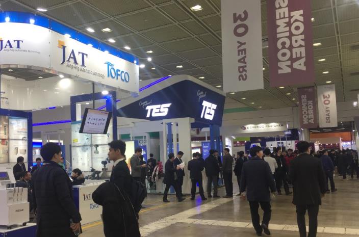
▲ View of the SEMICON 2017 exhibition hall.
Following a 2.6% growth in 2016, the materials market is projected to grow by 3.1% this year. China is expected to see a significant increase, growing by 7.2% compared to last year, followed by Taiwan (3.8%) and Korea (4.3%), which are expected to continue their growth. Overall, Southeast Asia is showing high growth, and China is also growing rapidly.
The packaging materials market is expected to grow at a rate in the 1% range due to overall growth but pressure to lower prices. In particular, the Chinese market, where global companies have increased facility investment, is projected to grow by 4.3% this year (4.60 billion in 2017).
Senior Manager Dan Tracy said, “As fab investments in 3D NAND increase, they are driving equipment investment as well. Equipment is expected to grow to the 9% range this year due to high order volumes in 2016, while materials are expected to see single-digit growth.”
Meanwhile, the Korean market accounts for 25% of the global 300mm production capacity and remains the largest share of the memory market. Samsung and SK Hynix together account for over 70% of the global DRAM market and over 45% of the NAND flash market. It is the number one consumer country for fab equipment.
3D NAND production capacity expanded by 800%
SEMI analyst Clark Chang focused on the investment situation in Chinese fabs.
Compared to 2015, 2D NAND investment is expected to decrease by 73% in 2017, while 3D NAND investment is projected to increase by 240%. During the same period, DRAM investment decreased by 19%, and analog investment fell by 27%. Foundry/MEMS is scheduled to grow by 285%, followed by increases in investment in Foundry (20%), MPU (35%), and Discrete/Power (11%). Accordingly, this year's investment scale is expected to reach $22 billion for Memory, $15 billion for Foundry, $3 billion for MPU, and slightly over $1 billion for Analog MEMS, Discrete, and Logic.
Analyst Clark Chang said, “As technology transitions from 2D to 3D NAND, 3D NAND production capacity is expected to expand by 800% between 2015 and 2017, followed by expansions in production capacity for products such as MEMS (25%), foundry (18%), and power (6%).”
China's fab investment more than doubled last year
China accounts for one-third of global investment in the semiconductor equipment market, to the extent that it has emerged as one of the top three regions. Investment share in assembly and packaging is estimated at 35% last year, while wafers are expected to reach 20% and testing slightly lower at around 12%. Although the wafer sector was not particularly high until 2012, it has shown a high growth rate since then. This is due to significant investments in fab projects and 3D NAND. Samsung's investment in Xi'an, China is also in the same context.
China's market share in materials is also continuing to grow. It is expected to hold a share of approximately 23% in assembly and packaging by last year, and the share in fab materials is projected to expand to 8%.
It is worth noting that China launched 20 new fab projects last year.
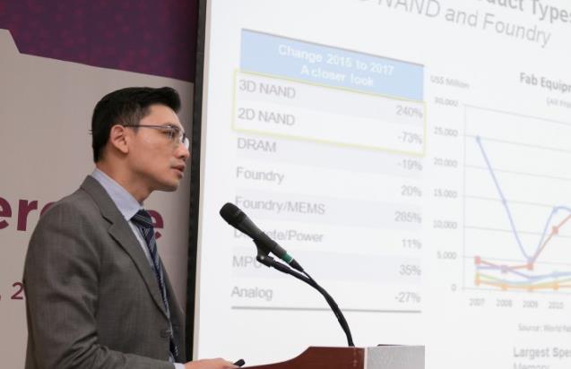
SEMI analyst Clark Chang said, “As not only Chinese companies but also foreign companies continue to invest, the investment momentum will continue.”
China's fab investment stood at the level of $60 to $70 billion until 2015, but it more than doubled last year. By product category, foundry and memory account for a large portion of new projects. While fab construction has decreased globally, China is expected to see a significant increase in investment in memory through 2019, and related fab investments are also projected to rise.
Chinese fab investment is expected to make a significant jump starting in 2018 and surpass $11 billion in 2019, a historical figure that has been shown by South Korea and Taiwan.
Chinese Fab Investment Expected to See a Significant Jump Starting in 2018
So, who is leading these investments? Chinese companies invested $2 billion last year and $5 billion in 2018, and are expected to increase further in 2019. Investment by foreign companies is also steadily growing. It is expected to exceed $5 billion in 2018 and $6 billion in 2019. China's production capacity is projected to rise from the current 14% to 17% in 2019 and to 20% thereafter. Overall capacity by product is expected to increase by more than 10% between 2015 and 2019, with foundry increasing by 14% and memory by 10%.
Analyst Clark Chang said, “Investment momentum will continue as not only Chinese companies but also foreign companies continue to invest,” adding, “China announced new IC promotion guidelines as a national policy in 2016, and government-level investment is increasing with the launch of the 13th Five-Year Plan.”
He continued, “China’s current problem is not a lack of capital, but a shortage of competent engineers. We need to recruit skilled engineers from Taiwan or Korea, and the recruitment of talent is particularly urgent in the flat panel display sector.” He added, “Furthermore, while there have been some successful aspects regarding outbound M&A (acquisition of overseas companies by domestic firms), regulatory issues still remain an obstacle.”
Comments 1
1 Comments:
Related news
The entire semiconductor market at a glance, Semicon Korea 2017 kicks off
SEMICON Korea, a leading semiconductor equipment and materials exhibition, opened on the 8th. SEMICON Korea, being held at Seoul COEX through the 10th (Friday), marks its 30th anniversary this year and welcomes visitors with an increased number of participating companies and diverse events. Since its launch in 1987 with 187 companies and 227 booths, SEMICON Korea is being held this year at its largest scale with 1,893 booths. The exhibition features participation from 500 companies across equipment and materials providers spanning the entire semiconductor industry supply chain, as well as companies in components, design, software, facilities, and various other sectors.
2017.02.08by 신윤오 기자
How Integris Solves Yield Concerns in Semiconductor Microfabrication
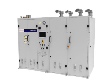
The new GateKeeper GPS product line uses advanced refining media to deliver best-in-class gas purification across a wider range of flow rates while reducing the equipment space required. Entegris has expanded its manufacturing capacity in Korea and now produces GateKeeper GPS systems in North America and Asia regions.
2017.02.08by 신윤오 기자
Edward Korea to Showcase New Anti-Corrosion Technology at SEMICON Exhibition
Edwards Vacuum (www.edwardsvacuum.com), which recently unveiled a new corrosion-resistant coating technology for critical components of vacuum pumps, exhibited the related technology at the SEMICON Korea exhibition, which runs through the 10th. Edwards, a specialized manufacturer of vacuum and gas processing solutions, provides key technologies for vacuum pumps used in harsh and highly corrosive semiconductor manufacturing processes.
2017.02.09by 신윤오 기자

Intel Unveils Next-Generation 'Core Ultra Series 3' and vPro Platform for Enterprise PCs
Intel has officially unveiled the "Intel Core Ultra Series 3" for next-generation enterprise PCs and the latest vPro platform, addressing a wide range of demands from enterprise notebooks to high-performance workstations.
2026.03.26by 배종인 기자

ROHM Launches ESD Protection Diode Compatible with High-Speed Interfaces of 10Gbps or Higher
Semiconductor specialist ROHM has developed the 'RESDxVx series' of ESD (electrostatic discharge) protection diodes capable of responding to next-generation high-speed data communication environments exceeding 10Gbps, simultaneously enhancing both signal quality maintenance required in high-speed interfaces and IC protection performance.
2026.03.26by 배종인 기자












쉽지많은 안겠죠.. ^^