



Samsung Electronics Expands Premium Market Through Mass Production of D-RAM for AI Systems
 Published2017.07.19 09:29
Providing optimal solutions including 'high capacity, ultra-high speed,·and ultra-low power consumption' for next-generation systems
Samsung Electronics is rapidly increasing production volumes of 8GB High Bandwidth Memory (HBM2) D-RAM, expanding supply not only to the supercomputer (HPC) market but also to network and graphics card markets. Samsung Electronics began mass production of 8GB HBM2 D-RAM in June of last year, pioneering the memory market for supercomputers utilized in artificial intelligence (AI) services, and has subsequently expanded the application scope of premium D-RAM to the existing high-end graphics card market.
The 8GB HBM2 D-RAM enables data transmission at 256GB per second, 8 times faster than the transmission speed (32GB/s) of existing graphics D-RAM (8Gb GDDR5, 8Gbps). This incorporates over 850 key patents including Samsung Electronics' 'ultra-high-density TSV design' and 'thermal management technology,' providing customers with optimal solutions including high capacity, ultra-high speed, and ultra-low power consumption for next-generation systems.
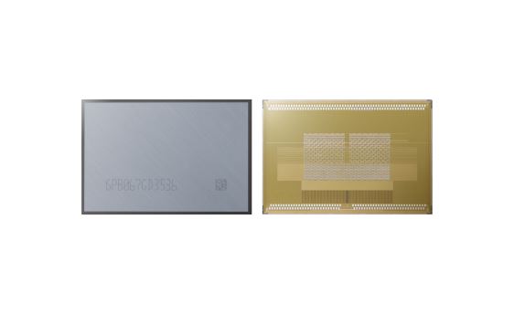
This product features a structure in which eight 8Gb HBM2 D-RAM chips (based on 20-nanometer process) are stacked on a single buffer chip, with over 5,000 fine holes drilled in each chip and vertically connected via over 40,000 'TSV bonding balls' using 'ultra-high-density TSV design technology.'
Particularly, when processing large volumes of information, if data transfer is delayed in some TSVs, the path is switched to alternate TSVs to prevent performance degradation and maintain optimal performance.
Samsung Electronics also developed and applied 'thermal management technology' that prevents specific areas of the chip from rising above the limit temperature during high-speed operation, thereby securing high levels of reliability.
Additionally, by providing twice the capacity in the same size as 4GB HBM2 D-RAM, it has contributed to overcoming performance limitations in artificial intelligence systems, and has approximately doubled the power consumption efficiency of next-generation systems.
Han Jae-soo, Senior Vice President of the Strategic Marketing Team at Samsung Electronics Memory Business Division, stated, "By expanding supply of 8GB HBM2 D-RAM, the only product being mass-produced in the industry, we have contributed to enabling customers to launch next-generation systems in a timely manner," and emphasized, "We will strengthen business cooperation with various global customers through the launch of next-generation HBM2 D-RAM product lineups in the future."
Samsung Electronics plans to expand mass production volumes of 8GB HBM2 products within the HBM2 product line to meet global IT customer requirements, increasing its proportion to over 50% in the first half of next year, and actively responding to premium D-RAM market demand.
Comments
Related news
Why the Semiconductor Market, Benefiting from DRAM and NAND Memory, Is a Worry in 2019
Gartner Inc. forecasted that global semiconductor revenue in 2017 would reach $38.6 billion, representing a 12.3% increase compared to the previous year. In the second half of 2016, the market showed strong performance as it secured growth momentum centered on commodity memory, which led to upward revisions of forecasts for 2017 and 2018. However, due to volatility in the memory market and increased production of DRAM and NAND flash memory, these forecasts are expected to be revised in 2019.
2017.04.17by 신윤오 기자
China's Shift from DRAM to NAND: Can Korea's 3D NAND Compete?
As the semiconductor market boom continues, Gartner, an IT market research firm, stated in a report on the 14th that "market growth is expected to continue through next year due to price increases and production volume growth in DRAM and NAND flash memory." IHS Markit senior research analyst Len Jelinek forecasted that "due to the large-capacity trend in IT devices, the amount of memory semiconductors installed in devices is increasing, and the memory semiconductor market growth rate will reach 30.3% this year." The system semiconductor market is expected to grow 10.5% year-over-year, and microcontroller units (MCU) are anticipated to show 6.7% growth driven by autonomous vehicle development. The overall memory market is projected to show growth through 2018, but from 2019 onwards, it is expected to slow due to variables such as China's government semiconductor industry policies. Mirae Asset Daewoo analyst Do Hyun-woo anticipated that the 2017 semiconductor equipment market will continue following last year's growth, with DRAM, foundry, and backend processes leading to overall 6% growth. The DRAM equipment market saw investment decrease at 23% last year, but this year investment is expected to increase by 15%, and due to memory market influence, investment will concentrate particularly in the second half. As Samsung Electronics and SK Hynix increase production volume of 18nm DRAM and invest in 17nm DRAM, equipment demand is predicted to increase. The NAND equipment market is expected to decline 4-5% compared to last year, as concentrated new capacity investments from Samsung Electronics, Toshiba, and Micron occurred in 2016. Samsung Electronics in particular invested heavily in 3D NAND flash at its Pyeongtaek plant last year, with plans to mass-produce 64-layer 3D NAND in the first half of this year. SK Hynix is preparing M14 3D NAND flash on the second floor of its Icheon plant this year, with plans to mass-produce 72-layer 3D NAND in the second half.
2017.05.01by 김지혜 기자
3D NAND on the Rise, Finding Processes and Materials to Solve Stacking Challenges
With 3D NAND supply volumes expected to surpass 2D NAND this year, interest is growing in the processes and materials required for stacking 3D NAND. On the 18th, the Semiconductor Electronic Materials Technology Conference (SMC, Strategic Materials Conference), hosted by the International Semiconductor Equipment and Materials Institute, was held under the theme "Scaling Challenges-The Future of Materials," discussing semiconductor material challenges for next-generation memory, market outlook for semiconductor materials, key process material technologies, and DRAM prospects. Sung-hyun Hong, Executive Director of Ram Research Korea, who presented, addressed the problems that arise as 3D NAND is stacked: "As the number of layers increases, the height becomes extremely high. If the structure is not harmonious, stress changes become severe. When stress becomes severe, the wafer bends, making handling difficult in subsequent processes."
2017.05.22by 김지혜 기자
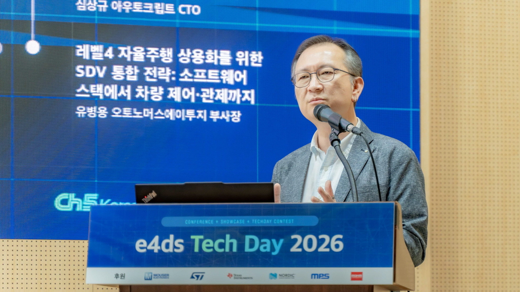
[e4ds Tech Day 2026 ⑨] Sim Sang-gyu, Autocrypt CTO: "In the Physical AI Era, Automotive Security Must Extend Beyond the Vehicle"
At e4ds Tech Day 2026, Sim Sang-gyu, CTO of Autocrypt, explained automotive cybersecurity strategies in the era of Physical AI and SDV (Software-Defined Vehicle). Automobiles are evolving as part of an ecosystem connected to AI, cloud, chargers, IoT, and robots, and he emphasized that the scope of security must expand beyond the vehicle interior to the entire connected environment. In particular, AI model tampering, adversarial attacks, OTA updates, and EV charger hacking were identified as major threats. He explained that response measures require zero trust, AI model integrity protection, intrusion detection, Security by Design and Default, and full lifecycle security management, and that proactive security system establishment beyond regulatory compliance is critical for securing future mobility competitiveness.
2026.10.12by 배종인 기자
NVIDIA to Invest $1 Billion in U.S. Science Over Next Five Years
NVIDIA has announced plans to invest $1 billion over the next five years to strengthen U.S. scientific and technological competitiveness. The company will enhance cutting-edge artificial intelligence research and development capabilities in key areas including quantum computing, healthcare, and energy security, while expanding support for higher education research institutions and cloud service providers. NVIDIA is participating as a major industry partner in the White House Office of Science and Technology Policy's Genesis Mission, and is promoting supercomputer construction in collaboration with national laboratories including Argonne and Los Alamos.
2026.10.12by 배종인 기자











