



Samsung Electronics Leads Global Semiconductor Microprocessing Technology in Hwaseong
 Published2018.02.23 19:11
We will contribute to the national economy through various mutually beneficial cooperation with related industries.
Samsung Electronics held a groundbreaking ceremony for the 'Samsung Electronics Hwaseong EUV Line' at its Hwaseong campus in Gyeonggi Province and has begun full-scale construction of the line. It is scheduled to be completed in the second half of 2019, followed by trial production, and will begin full-scale operation in 2020.
With the full-scale introduction of EUV (Extreme Ultra Violet) equipment—essential for overcoming the limitations of microfabrication processes—into this new line, it is expected to play a key role in Samsung Electronics maintaining its leadership in semiconductor microfabrication technology in the future.
The semiconductor industry has increased integration density and implemented fine circuits through process miniaturization, improving the performance and power efficiency of semiconductors. However, as miniaturization has recently progressed to single-digit nanometer scales, the introduction of EUV equipment with shorter wavelengths than conventional ArF (argon fluoride) light sources is necessary to implement more intricate circuits.
When EUV technology is fully commercialized, it can improve the performance and power efficiency of semiconductors, as well as reduce the number of process steps for circuit formation, thereby dramatically increasing productivity.
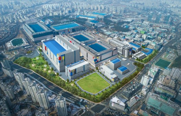
Samsung Electronics plans to use its Hwaseong EUV line to respond promptly to future demand in the advanced semiconductor market, which requires high performance and low power consumption for mobile, server, network, and HPC, and to lead the market for 7nm and smaller foundry advanced processes.
The initial investment for the Hwaseong EUV line is set at $6 billion by 2020, including construction costs, and Samsung Electronics plans to pursue additional investments depending on market conditions after the line begins operation.
The mutual growth between Samsung Electronics and Hwaseong City, which began with the development of the Samsung Electronics Hwaseong Campus in 2000, is expected to expand further with the construction of this new EUV line, solidifying its position as a mecca for the advanced semiconductor industry.
In his commemorative speech, Kim Ki-nam, President and Head of Samsung Electronics’ DS Division, stated, "With the establishment of this new EUV line in Hwaseong, the Hwaseong Campus will become the center of the semiconductor cluster connecting Giheung, Hwaseong, and Pyeongtaek," and added, "Samsung Electronics will contribute to the national economy through various win-win collaborations with academia, research institutes, and related industries."
관련뉴스

NI and Samsung Electronics Collaborate to Develop 5G NR Test UE for 28GHz
내쇼날인스트루먼트가 5G NR(New Radio)에 대한 5G 테스트 UE를 개발하기 위해 삼성전자와 협력한다고 밝혔다. NI와 삼성은 이번 협업의 성과로서 NI 테스트 UE와 통신하는 삼성의 28GHz 베이스 스테이션을 모바일 월드 콩그레스(MWC) 2018에서 최초로 공개 시연한다. 3GPP는 5G NR 표준의 초안을 2017년 12월 공식 발표했다. 새로운 5G 에코시스템 구축의 다음 주요 단계에서는 장비 및 디바이스 제조업체가 이러한 표준에 부합하는 구현성을 서로 테스트하여 상호운용 목표를 달성해야 한다. 상호운용성 디바이스 테스트(IODT)는 베이스 스테이션과 디바이스가 사전에 규정된 테스트 조건에서 5G 성능을 발휘할 수 있게 안정된 통신 링크를 설정하고 유지할 수 있는지를 판별한다.
2018.02.22by 김지혜 기자

Samsung Electronics and Qualcomm Partner to Produce 5G Chips Based on 7nm Foundry Process
Samsung Electronics has decided to cooperate with Qualcomm on 5G chip production based on the 7-nanometer foundry process (7LPP, Low Power Plus). Samsung Electronics plans to apply EUV (Extreme Ultra Violet), the next-generation lithography equipment, starting from the 7-nanometer process, and Samsung Electronics and Qualcomm have decided to expand their cooperative relationship to 7-nanometer following their collaboration on 14-nanometer/10-nanometer processes. Samsung Electronics is actively adopting EUV technology, including unveiling a 7-nanometer foundry process incorporating EUV lithography technology last May, and plans to continue overcoming the limits of ultra-fine processes to solidify its technological leadership.
2018.02.22by 김지혜 기자
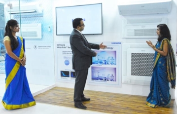
Will Samsung create a windless storm at ACREX 2018 in India?
삼성전자가 전 세계 30개국 600여개의 주요 공조 업체가 참가하는 인도 공조전(ACREX India 2018)에 참가해 ‘무풍에어컨’ 등 혁신적인 공조 솔루션을 대거 선보인다. 삼성전자는 바람이 직접 닿지 않는 ‘무풍 냉방’ 기술을 전기 사용량이 많은 상업용까지 확대한 ‘무풍 1Way, 4Way 카세트(천장형 실내기)’와 ‘시스템에어컨 360’ 등 무풍 에어컨 풀 라인업을 인도 시장에 공개한다. 올 상반기 인도 시장에 출시할 ‘무풍 4way 카세트’는 기존 제품 대비 블레이드 크기와 스윙 각도를 확대해 바람을 더 멀리 보낼 수 있어 넓은 공간도 빠르게 냉방해 준다. 또한, 사람의 위치를 감지해 바람 방향과 운전 모드를 변경하는 인감지 센서(MDS; Motion Detect Sensor)를 통해 에너지 효율을 극대화 시킨다.
2018.02.22by 김학준 기자

Intel Unveils Next-Generation 'Core Ultra Series 3' and vPro Platform for Enterprise PCs
Intel has officially unveiled the "Intel Core Ultra Series 3" for next-generation enterprise PCs and the latest vPro platform, addressing a wide range of demands from enterprise notebooks to high-performance workstations.
2026.03.26by 배종인 기자

ROHM Launches ESD Protection Diode Compatible with High-Speed Interfaces of 10Gbps or Higher
반도체 전문 기업 로옴(ROHM)이 10Gbps를 넘어서는 차세대 고속 데이터 통신 환경에 대응할 수 있는 ESD(정전기 방전) 보호 다이오드 ‘RESDxVx 시리즈’를 개발하며, 고속 인터페이스에서 요구되는 신호 품질 유지와 IC 보호 성능을 동시에 끌어올렸다.
2026.03.26by 배종인 기자











