



Multi-ADC interfacing method for power grid protection and control
 Published2018.11.18 07:02
Processor required to process electrical parameter calculations in real time
ADC interface to host processor must be isolated
As energy demand and consumption increases worldwide and the demand for green energy grows, power companies' strategies are also changing.
Power companies increase the efficiency of power transmission and distribution by improving the quality of power delivered to customers rather than increasing the amount of power produced. And they minimize downtime and reduce operating costs by extending the life of equipment through improved protection, monitoring, control, and automation while making the power system fault tolerant.
For example, fault-tolerant power systems can reduce fault currents, add intelligence to equipment using sensors, and connect to secondary protection equipment through communications. These devices can accurately detect fault currents and shorten the time to clear fault conditions. Remote operations can quickly and accurately identify fault locations to minimize downtime, shorten service recovery times to build redundancy and increase reliability, and data analytics can predict and prevent equipment failures early. Primary equipment such as transmission lines, power transformers, circuit breakers, and load switches play a critical role in maintaining power system integrity and uninterrupted power supply.
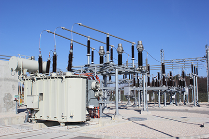
Power transformer installed in a substation
High-end secondary equipment also includes protection relays consisting of AC analog input modules and terminal devices (remote terminals, distribution terminals, feeder terminals, phase vector measurement units, etc.) for protection, monitoring, control, metering, and power quality analysis of primary equipment. Power companies are implementing and improving multiple protection algorithms and diagnostic techniques to protect equipment and the grid and to predict faults as early as possible.
Most sensors connected to these devices provide analog outputs proportional to the parameters they measure (voltage, current, temperature, etc.). This has led to a growing need to expand analog input channels in data acquisition systems to capture analog outputs from various sensors connected to primary equipment. Data acquisition refers to accurately measuring and processing electrical inputs such as voltage, current, and temperature. Therefore, the sampling rate must be selectable and the measured parameters must be processed in real time using a signal processor.
The key requirements for a high-performance data acquisition system are:
▲For multi-channel acquisition and redundancy, two or more multiple ADCs must be used to sample analog inputs from multiple sensors (4, 8, 16, or more).
▲To accurately measure electrical parameters, a 16-bit or higher precision SAR (successive approximation register) or delta-sigma ADC must be used.
▲It should be able to change the sampling rate based on the measurement or protection requirements according to the IEC 61850-9-2 standard (80 samples for protection and 256 samples for measurement), and it should be able to sample the input consistently. This allows the sampling rate to be maintained in accordance with the changing line frequency.
▲By simultaneously sampling inputs and maintaining the voltage and current phase angle relationship, the protection algorithm can be simplified and the trip time can be shortened.
▲In order to collect digital data sampled by ADC in real time, multiple ADCs must be interfaced to the host processor.
▲A host processor capable of simultaneously collecting samples from multiple ADCs and processing them in real time, including complex electrical parameter calculations, is required.
▲System costs must be optimized as system complexity increases.
▲To improve system performance and reliability, the ADC interface to the host processor must be isolated using a digital isolator.
There are several ADC architectures available. The most common are SAR or delta-sigma, and the interface between the ADC and the host processor can be either parallel or serial. Each host interface method has its own advantages. The serial interface is the simplest method because it allows multiple ADCs to be daisy-chained, but it has the disadvantage of low throughput. The parallel interface provides high throughput, but limits the ADC selection and increases cost and board complexity.
It also achieves higher throughput and maintains sampling flexibility by using multiple SPI (serial peripheral interface) ports with individually controllable chip select functions. The number of SPI ports required increases with the number of ADCs to be interfaced, and thus the real-time processing performance. Therefore, the host processor that can be used is limited because the SPI ports and real-time processing performance are limited.
As a result, some developers are adopting FPGAs that can use multiple SPI ports for ADC interfacing to achieve the required sampling flexibility and data throughput. However, this architecture requires additional application processors for human-machine and communication interfaces, which increases system cost and complexity.
TI's Interface for Simultaneous and Coherent Data Acquisition Using Multiple ADCs (PRU-ICSS) reference design simplifies data acquisition system design by using a 16-bit SAR ADC with integrated peripherals such as a programmable gain amplifier (PGA), precision reference and SPI serial interface, and a host processor with a dual-core programmable real-time unit and industrial communications subsystem (PRU-ICSS).
When interfacing multiple ADCs to a single processor is required, device and architecture selection is critical to successful design. Designers can simplify architecture selection and design for multichannel precision data acquisition systems requiring 16 or more precision analog input channels by using TI’s ICs and reference designs.
This article is a summary of the writings of Kallikuppa Sreenivasa, an engineer at Texas Instruments.
관련뉴스
SKT, 대구국가산단에 마이크로그리드 구축한다
SK텔레콤이 대구국가산단 마이크로그리드 2차 구축사업 주관사업자로 선정되어, 총 127억원 규모로 연말까지 40개 업체 대상 에너지 관리 솔루션을 적용할 예정이다.
2018.08.01by 이수민 기자
TI Introduces Two CAN FD Transceivers That Achieve Smaller, Stronger Isolation
Texas Instruments Korea has launched two isolated CAN FD transceiver products. The ISO1042 and ISO1042-Q1 isolated CAN FD transceivers provide high operating voltage and communication speed faster than the CAN standard. Additionally, they combine bus fault protection, CMTI, and low electromagnetic emission advantages in a compact package. TI's two transceivers protect low-voltage circuits and enhance communication throughput in industrial applications including electric vehicles and hybrid electric vehicles, as well as factory automation, power grid infrastructure, motor drives, building automation, and industrial transportation.
2018.11.08by 이수민 기자

TI Launches 60GHz Sensor Portfolio with Enhanced mmWave Sensing
Texas Instruments announced the launch of a new 60GHz sensor portfolio for industrial systems featuring high-resolution single-chip CMOS products to enhance mmWave sensor technology for industrial applications worldwide. The IWR6x millimeter-wave sensor enables industrial automation through on-chip processing capabilities and provides real-time decision-making and signal processing functions. The new 60GHz millimeter-wave sensor will feature antenna-on-package for the first time, addressing existing challenges related to RF design, reducing size by up to 75%, and lowering overall costs.
2018.11.10by 이수민 기자

Intel Unveils Next-Generation 'Core Ultra Series 3' and vPro Platform for Enterprise PCs
Intel has officially unveiled the "Intel Core Ultra Series 3" for next-generation enterprise PCs and the latest vPro platform, addressing a wide range of demands from enterprise notebooks to high-performance workstations.
2026.03.26by 배종인 기자

ROHM Launches ESD Protection Diode Compatible with High-Speed Interfaces of 10Gbps or Higher
Semiconductor specialist ROHM has developed the 'RESDxVx series' of ESD (electrostatic discharge) protection diodes capable of responding to next-generation high-speed data communication environments exceeding 10Gbps, simultaneously enhancing both signal quality maintenance required in high-speed interfaces and IC protection performance.
2026.03.26by 배종인 기자











