기사입력 2025.02.18 14:40
미국 상무부는 6일 SK하이닉스의 인디애나주 반도체 패키징 생산기지 투자와 관련해 미국 반도체법에 근거하여 최대 4억 5,000만 달러의 직접보조금과 5억 달러의 대출을 지원한다는 내용을 골자로 하는 예비거래각서(PMT, Preliminary Memorandum of Terms)에 서명했다.
2024-08-07 오후 3:38:58by 배종인 기자
글로벌 광학기업 자이스 코리아(대표이사 정현석)가 오는 8월28일부터 30일까지 수원컨벤션센터에서 열리는 제18회 차세대 반도체 패키징 장비재료 산업전(ASPS 2024)에 참가한다.
2024-08-21 오후 3:01:15by 배종인 기자
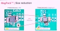
전력 설계에서 사이즈 이슈가 큰 비중을 차지한다. 이에 변압기 혹은 인덕터를 패키지에 결합해 EMI 이점 및 전력 밀도를 강화할 수 있는 마그네틱 패키징(MagPack) 기술이 공개됐다.
2024-09-02 오후 3:46:14by 권신혁 기자

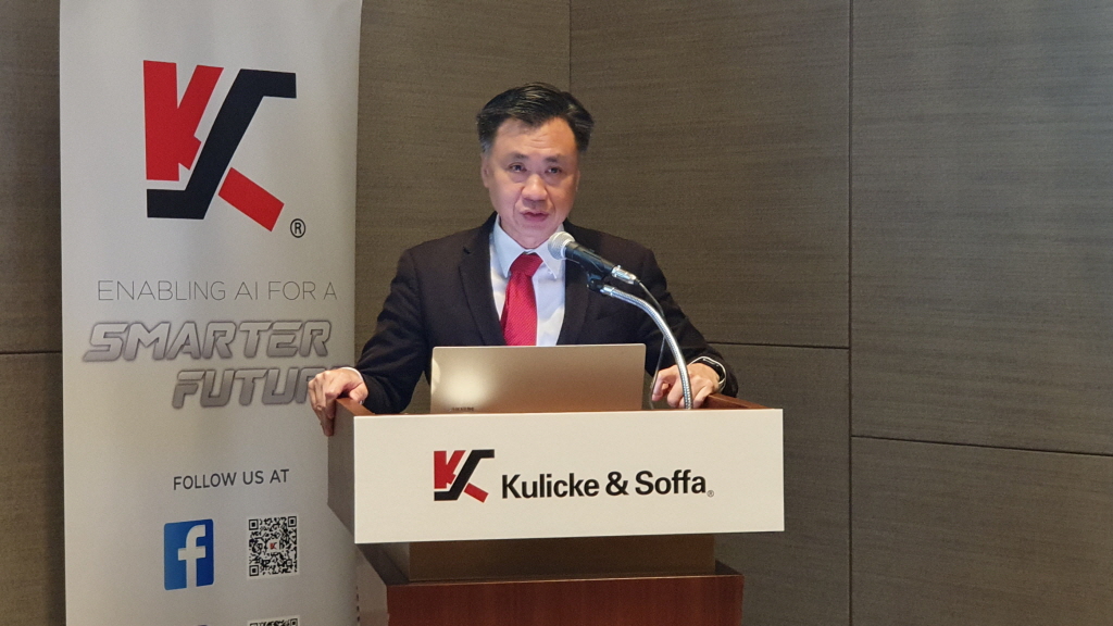
이강욱 SK하이닉스 부사장(PKG개발 담당)이 3일 SEMICON TAIWAN에서 ‘AI 시대를 대비하는 HBM과 어드밴스드 패키징 기술(HBM (High Bandwidth Memory) and Advanced Packaging Technology for AI Era)’을 주제로 발표하며, 2025년 HBM4 12단을 출시하겠다고 밝혔다.
2024-09-04 오전 9:32:01by 배종인 기자
.jpg)
반도체 및 첨단 웨이퍼 레벨 패키징(WLP) 애플리케이션을 위한 웨이퍼 처리 솔루션 선도 기업인 ACM 리서치(ACM Research)가 팬아웃 패널 레벨 패키징(FOPLP) 애플리케이션을 위한 Ultra C bev-p 패널 베벨 에칭 장비를 출시를 통해 구리 관련 애플리케이션의 공정 효율성과 신뢰성을 향상시켜 대형 패널 상에서 고정밀 특성을 지원한다.
2024-09-13 오전 11:20:08by 배종인 기자
텍사스 인스트루먼트(TI)가 전력 모듈을 위한 선도적인 마그네틱 패키징 기술인 MagPack™ 기술이 적용된 새로운 전력 모듈을 통해 기존 제품 대비 최대 50% 더 작아져 뛰어난 열 성능을 유지하면서 전력 밀도를 두 배로 향상시켰다.
2024-10-15 오후 2:34:01by 배종인 기자
.jpg)
미국과 일본 등 글로벌 반도체 산업이 표준화 활동에 선도적인 모습을 보이는 가운데 기술 선도와 종속의 갈림길에서 국내 반도체 산업의 생존을 위해 산학연이 힘을 합쳐 표준화 동향과 전망을 공유하는 자리가 마련됐다.
2024-11-18 오후 4:02:00by 권신혁 기자
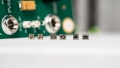
과학기술정보통신부 산하 한국기계연구원(원장 류석현) 자율제조연구소 반도체장비연구센터 송준엽 연구위원, 이재학 박사 연구팀과 한화정밀기계㈜, ㈜크레셈, ㈜엠티아이, ㈜네페스는 600㎜ 대면적의 패널 위에서 고집적 다차원(2.x/3D 반도체 패키징(SIP : System In Packaging)을 실현할 수 있는 FO-PLP 본딩 및 검사장비와 공정·소재기술 등 핵심 원천기술 및 특허 14건과 실용화 기술을 개발했다.
2024-11-27 오전 8:52:18by 배종인 기자

인텔 파운드리가 루테늄(Ru)을 활용해 정전 용량을 최대 25% 향상시키고, 칩 간 어셈블리 공정을 가능하게 하는 이기종 통합 솔루션을 활용해 처리량(쓰루풋)을 100배 향상 시킨 혁신적인 트랜지스터 및 패키징 기술을 공개했다.
2024-12-09 오후 12:59:47by 배종인 기자

[열린보도원칙] 당 매체는 독자와 취재원 등 뉴스이용자의 권리 보장을 위해 반론이나 정정보도, 추후보도를 요청할 수 있는 창구를 열어두고 있음을 알려드립니다.
고충처리인 장은성 070-4699-5321 , news@e4ds.com


