


Efficient USB-PD power design starts with component selection
 Published2021.01.06 14:35
ZVS/ZCS 가능한 플라이백 토폴로지 채택 권장
제품에 적합한 패키지 선택으로 EMI 저감 가능
오늘날 우리는 스마트폰, 태블릿, 랩톱, 무선 헤드폰을 비롯한 재충전 가능한 배터리로 구동하는 디바이스 등을 많이 사용하고 있다. 그러나 디바이스마다 충전기와 케이블을 따로 사용하는 것은 여간 불편한 일이 아니다.
만약 충전기와 케이블의 숫자를 하나로 줄일 뿐만 아니라 충전을 더 빠르게 할 수 있다면 어떨까? 이것을 가능하게 하는 것이 ‘USB-PD(Power Delivery)’이다. USB-PD는 모든 디바이스에 사용할 수 있는 충전 기술이다.
기술적 관점에서 폼 팩터, 충전 전력, 배터리 용량, 충전 시간 등이 계속 향상되고 있다. 여기에 보조를 맞추기 위해서는 전력 밀도와 효율을 높여야 한다. 이를 위해서는 다양한 토폴로지와 전력 기술을 사용할 수 있어야 한다.
고속 충전에 적합한 솔루션
먼저 토폴로지를 살펴보자. 충전기 디자인에 가장 널리 사용되는 플라이백은 다른 토폴로지에 비해서 비용이 낮고 설계가 쉽다. 그런데 전통적인 플라이백 컨버터는 에너지 저장을 위해서 큰 트랜스포머를 사용한다. 따라서 달성 가능한 최대 전력 밀도를 제한한다.
트랜스포머 크기로 인한 한계점을 극복할 수 있는 해결책은 스위칭 주파수를 높이는 것이다. 하지만 주파수를 높이면 기생 소자들의 에너지 손실(주로 트랜스포머 누설 인덕턴스)과 MOSFET 커패시턴스가 상당해진다.
높은 스위칭 주파수로 인한 문제들을 해결하기 위해서 변형된 방식의 소프트 스위칭 플라이백 토폴로지가 인기를 끌고 있다. 디지털 강제 주파수 공진(FFR)을 예로 들 수 있다. 이 토폴로지용으로 인피니언의 ‘XDPS21071 및 XDPS21081 디지털 컨트롤러’를 사용할 수 있다.
최근엔 GaN(질화갈륨) 기반 디바이스에 소프트 스위칭 플라이백을 결합하여 더 높은 스위칭 주파수를 달성하고, 고전력 밀도 어댑터의 한계점을 극복하고 있다. 기생 소자로부터의 에너지를 재활용하여 트랜스포머 크기를 줄인 것이다.
하지만 높은 스위칭 주파수는 나름의 문제를 수반한다. 빠른 스위칭 주파수는 EMI 측면에서 문제를 제기한다. 또한 시스템 비용에 민감한 시장에서 GaN 전력 스위치와 ZVS(제로 전압 스위칭) 컨트롤러 같은 특수한 디바이스는 가격이 비싸다.
비대칭 듀티 사이클 플라이백 컨버터는 플라이백과 포워드 컨버터를 결합한 것으로, 중간 스위칭 주파수로 동작하는 고밀도 어댑터 관련 문제들을 해결한다. 라인 및 부하 범위에 걸쳐서 ZVS와 ZCS(제로 전류 스위칭)을 가능하게 하므로 더 높은 효율을 달성할 수 있다.
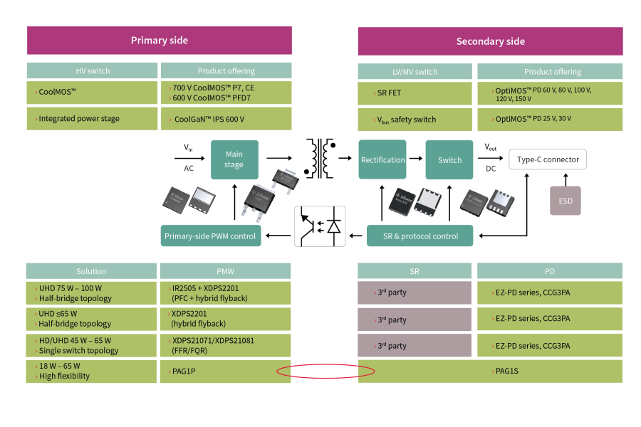
설계 엔지니어들이 각자 자신의 설계 목표를 달성할 수 있도록 인피니언은 고전압 및 저전압 전력 MOSFET, USB-PD 프로토콜 제품, 높은 전력 밀도를 달성하는 디지털 소프트 스위칭 컨트롤러를 비롯한 포괄적인 반도체 제품 포트폴리오를 제공한다.
적합한 USB-PD 컨트롤러 선택하기
충전기 시장은 대체로 최종 소비자 지향적으라 가격에 민감하고 성능을 중요시한다. 인피니언은 91% 이상의 효율을 요구하는 설계에는 가격 대 성능 비가 뛰어난 ‘2칩 PAG1 솔루션’을 권장한다.
해당 솔루션은 ‘PAG1P 일차측 스타트업 컨트롤러’와 동기 정류 제어와 USB-PD 프로토콜 제어를 통합한 ‘PAG1S 단일칩 이차측 컨트롤러’로 이뤄졌다. 특히 PAG1S는 프로그래머블 디바이스로서 유연성이 뛰어나다.
라인/부하 전압에 걸쳐서 컨버터가 스위칭하는 QR 골(valley) 값을 사용자가 세밀하게 조절할 수 있다. 그러므로 외부 하드웨어 부품을 변경할 필요 없이 시스템 효율을 최적화할 수 있다.
더 높은 92%의 효율을 원할 때는 디지털 기반 ‘XDPS21081 ZVS 컨트롤러’를 사용할 수 있다. 이 컨트롤러는 업계 최초의 플라이백 컨트롤러로서 일차측으로 ZVS와 간소화된 회로 및 경제적인 스위치를 사용해서 높은 효율을 달성한다.
음의 자화를 사용하는 FFR 스위칭 방식으로, 오늘날 골 스위칭 타입 컨트롤러와 관련된 손실을 낮추면서도 정주파수 스위칭 방식의 단순성을 희생하지 않는다. 그럴 뿐만 아니라 다수의 파라미터를 조절할 수 있어서 설계 유연성이 높다. 엔지니어는 각기 다른 시스템 사양에 따라서 자신의 디자인을 맞춤화할 수 있다.
더욱 높은 93%의 효율을 원할 때는 비대칭 플라이백 토폴로지가 권장된다. 인피니언에서는 이 토폴로지를 하이브리드 플라이백이라고 부른다. 컨버터가 혼합된 플라이백/포워드 모드로 동작하기 때문이다. 이 하이브리드 토폴로지는 자화 전류를 사용해서 일차 측 하프 브리지로 ZVS 및 동기 정류 스위치로 ZCS를 달성함으로써 최대의 변환 효율을 달성할 수 있다.
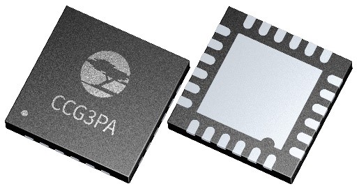

USB-C 프로토콜을 완벽하게 충족하는 것이 중요하게 요구될 때는 고집적 USB Type-C 포트 컨트롤러 ‘EZ-PD™ CCG3PA’가 권장된다. CCG3PA는 최신 USB Type-C 및 PD 표준을 충족하며, PC 전원 어댑터, 모바일 충전기, 차량 충전기, 파워 뱅크 애플리케이션에 사용하기에 적합하다.
인피니언에 인수된 싸이프러스 고유의 M0S8 기술을 기반으로 하며, 32비트 Arm® Cortex®-M0 프로세서, 64KB 플래시, 포괄적인 Type-C USB-PD 트랜시버, Type-C 포트에 필요로 하는 모든 종단 저항, 전압(VBUS) 레귤레이션에 필요로 하는 피드백 제어 회로, 시스템 차원의 ESD 보호 기능을 포함한다. 24핀 QFN 및 16핀 SOIC 패키지로 제공된다.
적합한 USB-PD 전력 스위치 선택하기
인피니언은 전원 효율을 높이는 여러 고성능 전력 스위치 제품을 제공한다. 최근에는 경제적인 가격대로 최신 충전기 설계에 적합한 일련의 제품들을 출시했다.
‘600V CoolMOS™ PFD7 시리즈’와 ‘700V/800V CoolMOS™ P7 시리즈’는 경쟁력 있는 가격대로 향상된 기술을 사용해서 스위칭 손실과 전도 손실을 낮춘다. 또한 게이트-소스 제너 다이오드를 통합하여 ESD 보호와 시스템 신뢰성을 높인다.
총 게이트 전하(Qg)가 낮고 MOSFET 출력 커패시턴스로 에너지 저장이 낮으므로(하드 스위칭 시에 매 사이클에 소모되는 에너지(Eoss)) MOSFET의 스위칭 손실을 높인다. 매 스위칭 사이클에 소모되는 이 총 전하를 낮춤으로써 경부하 시 시스템 효율을 높인다.
향상된 기술은 디바이스 전도 손실을 낮춤으로써 디바이스 온도 계수를 높인다. MOSFET의 RDS(on) 정격은 25℃일 때에 관한 것으로서, 동작 시에는 접합부 온도가 그보다 높게 상승한다.
이전 세대 C6 기술과 비교해서 PFD7/P7 시리즈는 100℃일 때 RDS(on)이 10% 감소함으로써 전도 손실을 그만큼 낮춘다. 125℃일 때 통상적인 산업 표준으로는 RDS(on)이 데이터 시트값의 2배인데, 최근에는 이것을 1.9배로 낮췄다.
전도 손실과 스위칭 손실을 이처럼 높이므로, RDS(on)이 더 높은 MOSFET을 사용해서 전체적인 시스템 비용을 낮추거나 또 다르게는 전반적인 시스템 스위칭 주파수를 높여서 폼 팩터를 줄이고 수동 부품 비용을 낮출 수 있다.
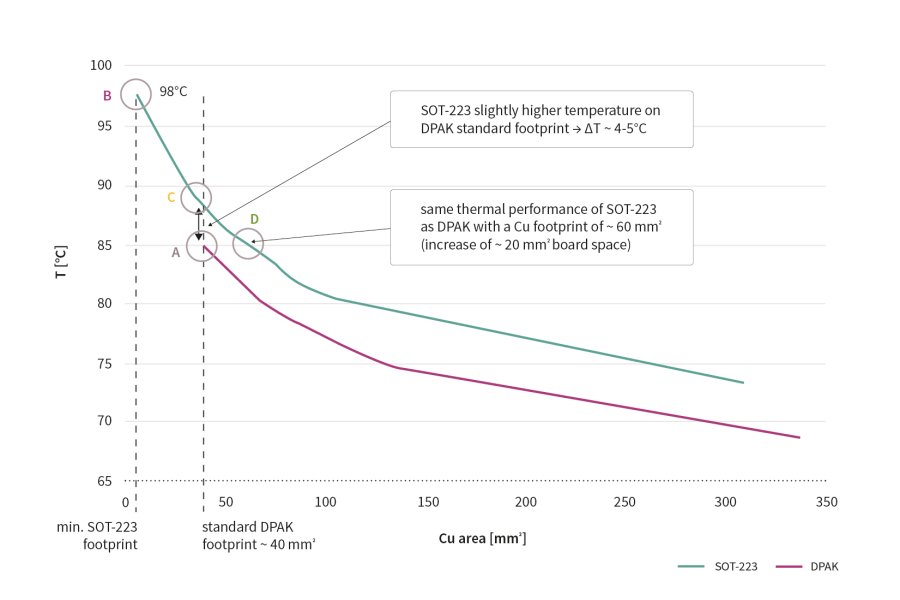
SOT-223 패키지는 DPAK과 비슷한 열 성능을 달성할 수 있다
[그래프=인피니언]
적합한 패키지 선택 또한 USB-PD 충전기 솔루션의 성능을 높일 수 있다. 경제적인 SOT-223 패키지를 예로 들 수 있다. 이 패키지는 더 낮은 가격으로 DPAK을 바로 대체할 수 있다.
ThinPAK 패키지는 소스 인덕턴스가 매우 낮고, 별도의 드라이버 소스 배선을 사용해서 깨끗한 게이트 신호를 제공하고, 향상된 정류 루프(MOSFET, 다이오드, 커패시터)를 사용해서 극히 낮은 기생 인덕턴스를 달성한다.
VDS 오버슈트를 낮추는 데 도움이 되는 ThinPAK 패키지는 전력 MOSFET을 더 빠르고 효율적으로 스위칭할 수 있으며 스위칭 동작과 EMI 측면에서 더 수월하게 취급할 수 있다.
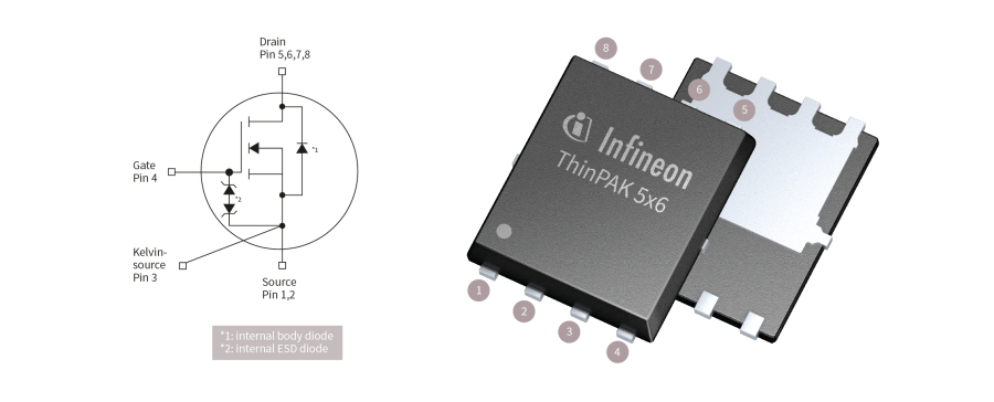
낮춰 VDS 오버슈트를 낮춘다 [그림=인피니언]
이차측으로는 USB-PD 충전기의 동기 정류와 부하 스위칭용으로 ‘OptiMOS™ PD 시리즈’를 사용할 수 있다. 이 제품군은 RDS(on)이 낮고, 스위칭 손실이 낮고, 게이트 전하, 출력 전하, 역 복구 전하가 낮은 MOSFET 제품들을 제공한다.
또한, 로직 레벨 버전 제품들을 제공하므로 4.5V로 최대로 구동하거나 MCU로 곧바로 구동할 수 있으므로 애플리케이션의 부품 수를 줄일 수 있다. PQFN 3.3 × 3.3 및 SuperSO8 패키지는 USB-PD 충전기의 크기를 축소할 수 있다.
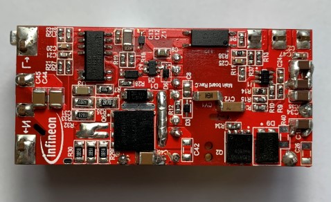
한편, 인피니언은 쉽게 사용 가능한 ‘65W 20W/in3(50CC) USB-PD 디지털 FQR XDPS21081 레퍼런스 설계’를 제공한다. 이 실리콘 기반 솔루션은 견고성, 높은 전력 밀도, 낮은 가격대, 손쉬운 설계를 특징으로 한다. 규격화된 부품들을 사용해서 생산 복잡성을 낮춘다.
인피니언, USB-PD 위한 포괄적 솔루션 제공
USB-PD 프로토콜이 충전기 시장을 통일하고 있다. 인피니언은 고밀도 USB-PD 충전기 설계용으로 경제적인 가격대의 포괄적인 솔루션 포트폴리오를 제공한다. 다양한 전력 MOSFET, 컨트롤러, 레퍼런스 디자인을 제공하므로 설계 엔지니어는 자신의 설계에 적합한 제품을 쉽게 고를 수 있다.
디지털 기반 ‘XDPS21081 XDP™ 컨트롤러’는 ZVS/ZCS 동작을 위한 새로운 제어 기법을 사용해서 플라이백 컨버터를 향상한다. 맞춤화된 수퍼정션 고전압 ‘CoolMOS™’ 및 저전압 ‘OptiMOS™’ 제품군은 경제적인 가격대의 전력 스위치 솔루션을 제공하여 최종 제품 가격을 낮출 수 있다.
다양한 구성의 USB-C 프로토콜 컨트롤러 제품은 유선 통신 기능을 향상한다. 유연하게 조절 가능한 레퍼런스 디자인을 사용해서는 원하는 USB-PD 충전기 솔루션을 쉽고 빠르게 개발할 수 있다.
이 기사는 인피니언의 팀 후(Tim Hu) 글로벌 저전력 SMPS 애플리케이션 디렉터가 저술한 ‘USB-PD를 위한 인피니언의 포괄적인 솔루션(Solved Problems Look Easy - USB-PD Solutions)’이란 제목의 글을 정리한 것입니다.
Comments
Related news
Maxim Unveils Two USB Type-C High-Speed, High-Power Charging Solutions
As portable devices adopt new technologies such as 5G network connectivity and 4K video, many products are transitioning from single-cell to dual-cell series architectures. This has driven increased demand for USB Type-C Power Delivery and high-power charging of 25W and above. In response, Maxim announced the launch of two USB Type-C PD solutions: 'MAX77958' and 'MAX77962'.
2020.08.12by 강정규 기자

Infineon Introduces Solution for Verifying Qi 1.3 Wireless Charging Certification
Inductive wireless charging devices have been rapidly spreading with convenience at the forefront. However, unauthenticated chargers can not only shorten the battery life of devices but also potentially harm users in the worst cases. In response, Infineon has unveiled the "OPTIGA Trust Charge" product line, an embedded security solution for safe wireless charging.
2020.11.17by 강정규 기자
ADI Announces 80V Buck-Boost I2C Battery Charge Controller
ADI has launched the LT8491 buck-boost battery charging controller that supports MPPT temperature compensation and I2C interface functionality for telemetry and control applications. It operates regardless of whether the input voltage is higher than, lower than, or equal to the regulated battery float charge voltage. It offers three selectable constant current constant voltage charging profiles, making it suitable for charging various types of chemical batteries.
2020.12.15by 강정규 기자

Intel Unveils Next-Generation 'Core Ultra Series 3' and vPro Platform for Enterprise PCs
Intel has officially unveiled the "Intel Core Ultra Series 3" for next-generation enterprise PCs and the latest vPro platform, addressing a wide range of demands from enterprise notebooks to high-performance workstations.
2026.03.26by 배종인 기자

ROHM Launches ESD Protection Diode Compatible with High-Speed Interfaces of 10Gbps or Higher
Semiconductor specialist ROHM has developed the 'RESDxVx series' of ESD (electrostatic discharge) protection diodes capable of responding to next-generation high-speed data communication environments exceeding 10Gbps, simultaneously enhancing both signal quality maintenance required in high-speed interfaces and IC protection performance.
2026.03.26by 배종인 기자











