



[Power Special Feature I] EMI Avoidance Driving Circuit Techniques for Building High-Power GaN Switching Devices!
 Published2021.03.31 11:31
스위치들의 게이트 비대칭이 고주파 발진 요인이 되기도
전원 컨버터 사용에 있어 효율을 조금이라도 올리는 것이 제품 성능의 차이를 만들 수 있거나, 전력 밀도가 중요한 애플리케이션을 사용하고 있다면, 기존 실리콘 MOSFET 에서 갈륨 나이트라이드(GaN) 트랜지스터로의 전환을 고려해 볼 수 있다. 그러나 실리콘과 마찬가지로 GaN도 생산 다이 크기에 한계가 있어 하나의 디바이스가 처리 가능한 전류 용량에 제한이 있다.
출력 전력을 높이기 위해서는 대체적으로 스위칭 디바이스의 병렬 연결을 주로 사용하고 있지만, 설계시 문제가 발생될 소지가 있기에, 다양한 기술적 고려가 요구된다.

GAN 스위칭 디바이스를 병렬로 연결할 때 고려사항
스위칭 디바이스를 병렬로 동작시킬때 가장 먼저 고려해야 할 것은 사용하고자 하는 디바이스의 RDS(on) 즉 병렬 스위치들 간의 균등한 정적 전류 흐름 공유를 통한 디바이스 매칭이다.
두 번째 고려사항은 동적 스위칭이다. 스위치들의 게이트로 대칭을 이루지 않으면 디바이스 간에 전류 공유가 불균등해질 뿐만 아니라, 전류 흐름에 회로 기생 성분들이 혼합되어, 바람직하지 않은 고주파 발진을 일으킬 수 있다. 이는 전자기 적합성(EMC) 요건을 미충족 시키며, 심할 경우 스위치 자체의 손상을 야기할수도 있다.
실리콘 MOSFET의 병렬 동작에 대해서는 잘 알려져 있으나, GaN HEMT(High Electron Mobility Transistor)는 단일 디바이스를 구동하는 것조차 이해가 부족한 실정이다. 그런데다 GaN 디바이스는 스위칭 속도가 매우 빠르므로, 병렬로 작동하고자 할 경우에는 이들 전력 트랜지스터에 대해 철저한 이해를 필요로 한다.
구동 회로 설계
인피니언의 CoolGaN™ 600V HEMT 같은 디바이스는 게이트 하단에 p형 불순물 GaN을 사용한다. 그러면 디바이스의 임계 전압이 양의 값이 되며, 이 값은 통상적으로 대략 1.0V~1.5V로 매우 낮다. 결과적으로 게이트가 순방향 전압은 약 3.0V이고 저항은 수 Ω에 이르는 pn-다이오드를 형성한다. 그러면 구동 회로가 기존 MOSFET에 사용되는 것과 많이 다르다.
.png)

CoolGaN™ 트랜지스터의 게이트 입력은 게이트 커패시턴스 CG와 병렬로 순방향 전압 VF가 약 3.5V인 다이오드로 생각할 수 있다. 이 다이오드가 디바이스 구동을 까다롭게 한다. 왜냐하면 밀러 플래토에 도달했을 때 게이트 노드가 VF에 가까운 값으로 클램프되기 때문이다. 그러므로 하드 스위칭 애플리케이션으로 트랜지스터를 턴오프하기 위해서 음의 전압이 필요하다. 또한 정상 상태일 때와 오프/온 전이 시에 필요한 구동에 차이가 있다.
그림 1의 회로는 이러한 문제를 쉽게 해결할 수 있도록 돕는다. Ron이 Con과 CGS를 충전하도록 임피던스가 낮으면서 빠른 AC 경로를 제공한다. 이렇게 되도록 하기 위해서는 구동 전압 VS가 VF의 두 배 이상이 되어야 한다(8V~10V가 통상적). 그런 다음에는 RSS를 통해서 병렬 DC 경로가 형성된다. 그러므로 적정하게 설계했을 때 온(on) 전이 전류는 Ron에 의해서 결정되고, RSS는 정상 상태 다이오드 전류를 결정한다.
게이트가 턴오프되면 CGS와 Con의 전하가 빠르게 평형을 이룬다. 이렇게 되기 위해서는 Con을 CGS보다 크게 해야 한다. 전하에 차이가 있으면 게이트 전압 VG가 음이 되고, 그러면 하드 스위칭 애플리케이션으로 트랜지스터를 턴오프시킨다.
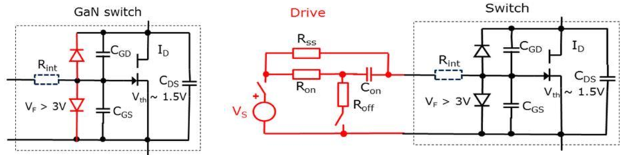
CoolGaN™ HEMT를 병렬로 동작할 때는, 실리콘 MOSFET 애플리케이션에 통상적으로 사용되는 표준 게이트 드라이버와 함께 각기 트랜지스터의 게이트에 이 동일한 RC 구동 네트워크를 사용할 수 있다. 절연형 EiceDRIVER™ 1EDI20N12AF 같은 단일 게이트 드라이버가 필요하며, 소스(OUT+)와 싱크(OUT-) 출력을 사용해서 트랜지스터 턴온과 턴오프를 구현할 수 있다.
게이트 드라이버에 절연형 12V 전원을 사용하면, 이 전원이 양 및 음의 전원으로 분할되고 음의 전원은 -2.5V로 레귤레이트된다. 이렇게 해서 트랜지스터 게이트 임계값을 넘지 않도록 하고 역 전도 손실을 최소화하도록 한다. 또한 낮은 듀티 사이클로도 게이트 전압을 잘 제어하고, RC 구동 네트워크가 0V가 되지 않도록 한다.
대체 전류 경로가 미치는 영향
각기 트랜지스터로 각각 RC 구동 회로를 사용하더라도 여전히 공유 전류 경로가 게이트 드라이버 루프로 방해를 일으킬 수 있다(그림 2). 이상적으로는 모든 전류가 드레인에서 소스로 의도한 경로로 흘러야 할 것이나, 불가피하게 일부 전류가 켈빈 소스 경로로 흐를 수 있다.
이들 경로가 임피던스와 배선이 동일하지 않으면 eT 게이트 루프로 VGS 전압이 달라질 수 있다. 게이트로 수 mV만 차이가 나더라도 전류 공유가 수 암페어 불균등해질 수 있으며, 두 트랜지스터 간에 스위칭할 때 심각한 발진이 발생될 수 있다.
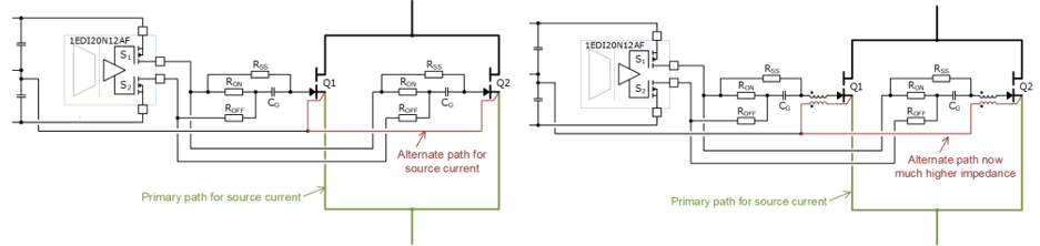
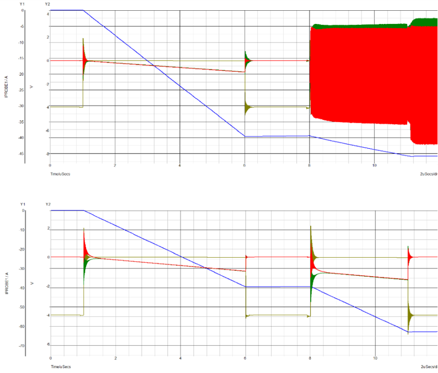
켈빈 소스 경로로 고 임피던스 공통 모드(CM) 경로를 사용해서 이 문제를 해결할 수 있다. 게이트와 해당 켈빈 소스 드라이버 리턴 경로 사이에 CM 인덕터를 사용하고 여기에 1Ω 저항을 더함으로써 게이트 구동 루프로 소량의 누설 인덕턴스만 발생되도록 할 수 있다. 한편으로 공유 전류 경로는 양쪽 인덕터의 차동 CM 인덕턴스가 된다. 게이트 드라이버 동작을 방해하지 않도록 하기 위해서는 인덕터를 신중하게 선택해야 한다. 그림 3에서는 SIMetrix 시뮬레이션 결과를 통해서 CM 인덕터가 미치는 영향을 알 수 있다.
전원 컨버터에 와이드 밴드갭(WBG) 기술이 기존 실리콘 MOSFET을 대체하고 있다. 그러나 기존 실리콘 MOSFET 과 달리 게이트 구동이 다른 GAN 전력 트랜지스터는 아직 많은 설계 엔지니어에게 여전히 낮선 디바이스중 하나이다. 특히 GaN HEMT의 경우 넓은 주파수 범위에서 큰 출력 전력을 요구하는 군수 및 민간용 레이다 통신 시스템의 고출력 마이크로웨비나 전력증폭기에 많이 사용되고 있어, EMC 요건 충족이 되지 않을 경우, 스위치 자체 손상뿐 아니라, 연계된 시스템에 까지 영향을 미칠수 있다.
실리콘 MOSFET이든 GaN 트랜지스터이든 병렬 구성은 높은 전원 출력 구성을 위한 기본적 설계 방식이다. 그러나 각 디바이스의 게이트 구동이 다르다는 점에 대한 이해와, 간단한 몇가지 구동 회로 설계 고려사항을 유의 한다면, 좀더 쉽고 빠르게 EMC요건에 적합한 고출력의 디바이스 병렬 구성이 가능하다.
참고자료
- Server 및 통신용 SMPS 적용 사례
- 초고속 무선 충전 애플리케이션 적용 사례
- Class D Audio Amplifier 적용 사례
- GaN HEMT Datasheet 확인하기
- CoolGaN 트랜지스터 동영상 강의 시청하기

Comments
Related news
Infineon Launches 'Si+SiC' 650V Hybrid IGBT Family
Infineon launches a 650V CoolSiC hybrid IGBT discrete product family. The product family combines 650V TRENCHSTOP 5 IGBT technology with a unipolar Schottky barrier CoolSiC diode. With high switching frequency and low switching loss, it is suitable for DC/DC converters and PFC, and can be utilized in battery charging infrastructure, energy storage solutions, solar inverters, UPS, server and telecom SMPS applications.
2021.02.18by 강정규 기자
Infineon Supplies GaN Solutions to Improve Power Efficiency in Communication Equipment
Infineon's CoolGaN 600V e-mode HEMT for telecom power supplies has been adopted in Delta's DPR 3000E EnergE rectifier. Infineon's GaN HEMT meets JEDEC standards, provides over 15 years of lifespan, and is suitable for industrial telecom and server SMPS applications. Supplied in a DFN8x8 package, it has raised the energy efficiency of Delta's rectifier to 98%.
2021.03.11by 강정규 기자
Infineon Unveils 2nd Generation StrongIRFET 80/100V MOSFET
Infineon has unveiled StrongIRFET 2, its next-generation 80V and 100V power MOSFET technology. It is optimized for both low and high switching frequencies, offering high design flexibility as it can be used in diverse applications. Compared to the previous generation, RDS(on) has improved by 40%, and Qg is reduced by over 50%, delivering higher power efficiency and enhanced overall system performance.
2021.03.19by 강정규 기자

Intel Unveils Next-Generation 'Core Ultra Series 3' and vPro Platform for Enterprise PCs
Intel has officially unveiled the "Intel Core Ultra Series 3" for next-generation enterprise PCs and the latest vPro platform, addressing a wide range of demands from enterprise notebooks to high-performance workstations.
2026.03.26by 배종인 기자

ROHM Launches ESD Protection Diode Compatible with High-Speed Interfaces of 10Gbps or Higher
Semiconductor specialist ROHM has developed the 'RESDxVx series' of ESD (electrostatic discharge) protection diodes capable of responding to next-generation high-speed data communication environments exceeding 10Gbps, simultaneously enhancing both signal quality maintenance required in high-speed interfaces and IC protection performance.
2026.03.26by 배종인 기자











