



"Utilizing SiC MOSFETs, Design Optimization is Essential"
 Published2021.06.25 14:56
Utilizing SiC MOSFETs, Component Selection and Gate Resistance Value
It depends on the tuning, so you should be familiar with double pulse tests, etc.
Improving power efficiency is the goal of all engineers designing electronic devices. High-performance electronic devices that operate stably for a long time are highly competitive in the market, and the demand is even greater these days when environmental protection and ESG management are hot topics.
To this end, many electronic device manufacturers are incorporating wide-bandgap (WBG) devices based on silicon carbide (SiC) and gallium nitride (GaN), which allow for higher voltages and lower losses than existing silicon (Si)-based devices, into their products.
MOSFET is an essential component of electronic devices, and recently, many products using SiC materials have been released. SiC MOSFETs are more expensive than Si devices, but they have the advantages of high efficiency and small size. However, if the system design is not optimized, these advantages cannot be utilized, and even the reliability of the system is damaged. In this case, there is no point in adopting them.

Infineon Korea's Industrial Power Control division provides component solutions used in industrial products such as commercial inverters and ESS. Here, we asked Deputy Manager Lee Geon-ho, who is in charge of technical support, about how to effectively adopt and utilize SiC MOSFETs.
Q. What is the trend of SiC products in the MOSFET market?
A. SiC MOSFETs are getting more attention in the IGBT market than in the MOSFET market. The biggest advantage of SiC MOSFETs is that they basically have low switching losses, which allows for high-speed switching, but MOSFETs themselves have low switching losses. Therefore, the advantages of SiC MOSFETs over Si MOSFETs are smaller than the advantages of SiC MOSFETs over IGBTs.
Q. What is the most difficult part of designing a SiC MOSFET?
A. Since SiC MOSFETs perform high-speed switching, gate malfunction due to c*dv/dt is a major problem. The most typical way to solve this is to use negative voltage at the gate terminal. Since the lifespan of SiC MOSFETs decreases as the negative voltage increases, c*dv/dt should be solved with the smallest possible negative voltage.
Therefore, the selection of gate resistor is very important. Infineon devices with threshold voltages 1~2V higher than those of other companies can create an environment where small gate resistors can be used, and can have great advantages in switching frequency and loss.
Q. How do you evaluate the suitability of SiC MOSFET devices?
A. In short, there are two things to verify. One is whether the turn-off spike voltage exceeds the withstand voltage. The worst case scenario is when the current condition is large, so a short-circuit test should be performed in parallel. The other is the c*dv/dt check. The worst case scenario is when the current condition is small.
Q. There is a 'double pulse test' during the suitability test. What is it?
A. The biggest difference between a double pulse test and a general load test is whether the measurement is made under specific current conditions or at different currents each time.
The load current changes in real time, such as a sine wave. When the gate resistance is 10Ω, it is measured at 10A, and when the gate resistance is 5Ω, it is measured at 9A or 11A. It is difficult to judge whether the improvement is real or if it appears to be improved because the current is lower.
It is also difficult to measure switching losses such as Eon and Eoff at the selected gate resistance value because it is not known whether the load current is the current of the relevant element or the current flowing to other elements.
In the case of SiC MOSFETs, the unit price is high, so losses must be optimized to take advantage. However, if you cannot measure the exact Eon, Eoff values, or if you cannot use a lower resistance but use a resistor with a large margin, it can lead to losses.
In particular, in the case of turn-off spike voltage, it can be linked to damage or stability of the device in terms of reliability, so it is necessary to select the gate resistance under accurate conditions and measure the switching loss, and the optimized test for this is the double pulse test.
Q. What are the strengths of Infineon’s SiC MOSFET and driver IC products?
A. SiC MOSFETs and driver ICs each have two advantages.
First, Infineon SiC MOSFETs have a threshold voltage of 4.5 V. In the field, the design is adjusted to the minimum threshold voltage value in the data sheet, and the minimum standard is also 3.5 V. Considering that products in the 1 V range are mainstream, Infineon’s threshold voltage is more than twice that of other companies.
In addition, Infineon guarantees the short circuit capability. Few companies other than Infineon guarantee this in their datasheets, and they guarantee 3us for discrete standards such as TO-247 and 2us for modules.
If a premium system that uses SiC MOSFETs cannot guarantee reliability and stability, a slightly higher efficiency is meaningless, so we focused on improving this.
Another great advantage of Infineon's drive ICs is their soft turn-off capability. Infineon driver ICs are normally hard-off to minimize losses and only turn off slowly when a short circuit occurs.
The turn-off spike voltage is worst when short-circuit current flows. If you design it so that the withstand voltage is not exceeded, you will have to use a gate resistor with a large loss at turn-off even at normal times. The soft turn-off function prevents this.
It is no exaggeration to say that this feature was created for SiC MOSFETs.
The second is that the DESAT filter time can be adjusted. Most devices have a filter time of several hundred nanoseconds, which is a long enough time for false detections due to noise. However, devices that can adjust the DESAT filter time up to 4 microseconds can safely protect the system from DESAT false detections.
Q. Are there any Infineon solutions related to SiC MOSFETs that you would like to introduce?
A. Infineon provides customized thermal coupler samples. Discrete products such as TO-247, which have a single chip, are easy to measure and manage temperature, but for modules with multiple components, it is difficult to measure the junction temperature and manage the temperature. To this end, we provide customized module samples that can measure the junction temperature by attaching a temperature sensor on the chip. Since the junction temperature can be measured during actual operation, there is a great advantage in terms of temperature management.
Q. What are Infineon's goals and plans in the SiC MOSFET market?
A. Currently, Infineon’s discrete SiC MOSFET lineup supports up to 27 mΩ for 650 V products and up to 30 mΩ for 1200 V products. Infineon plans to launch products supporting even smaller RDS(on), that is, single-digit mΩ, in the next year or the year after. Separately, for module solutions, it is planned to reach 2 mΩ, so that it will gradually provide SiC MOSFET solutions suitable for high-current applications.
Infineon's webinar on diagnosing the status of systems that use SiC MOSFETs and how to tune gate resistance values will be held on Thursday, July 22nd at 10:30 AM. The webinar will demonstrate an example using a board with SiC MOSFETs in a half-bridge structure. Since double pulse testing is performed on only one phase, whether single or three phases, the half-bridge board can be used to sufficiently conduct tests.
Comments
Related news
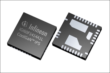
Infineon Launches GaN IPS Family for Mid-to-Low Power Applications
Infineon has strengthened its WBG power device portfolio by launching a new CoolGaN IPS product family. The first product, the 600V CoolGaN IGI60F1414A1L half-bridge IPS, is suitable for medium to low power applications such as chargers, adapters, and SMPS.
2021.05.18by 강정규 기자
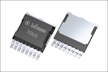
Infineon Launches Two New OptiMOS™ Power Semiconductor Products
Infineon Technologies (Chief Executive Officer Lee Seung-soo, Korea) has unveiled a new power MOSFET package that meets diverse design requirements of power system designers and enables maximum performance in minimal space.
2021.06.16by 명세환 기자
.jpg)
ROHM Unveils AC/DC Converter with Integrated 1700V SiC MOSFET
Auxiliary power supplies for high-power industrial equipment have faced difficulties in achieving low power consumption due to the adoption of low breakdown voltage Si MOSFETs or high-loss IGBTs. In response, Rohm has developed the BM2SC12xFP2-LBZ AC/DC converter IC, which incorporates a 1700V breakdown voltage SiC MOSFET. The new product integrates the SiC MOSFET and auxiliary power supply control circuit in a TO263-7L surface mount package, making it suitable for low-power AC/DC converter development.
2021.06.17by 이수민 기자

Intel Unveils Next-Generation 'Core Ultra Series 3' and vPro Platform for Enterprise PCs
Intel has officially unveiled the "Intel Core Ultra Series 3" for next-generation enterprise PCs and the latest vPro platform, addressing a wide range of demands from enterprise notebooks to high-performance workstations.
2026.03.26by 배종인 기자

ROHM Launches ESD Protection Diode Compatible with High-Speed Interfaces of 10Gbps or Higher
Semiconductor specialist ROHM has developed the 'RESDxVx series' of ESD (electrostatic discharge) protection diodes capable of responding to next-generation high-speed data communication environments exceeding 10Gbps, simultaneously enhancing both signal quality maintenance required in high-speed interfaces and IC protection performance.
2026.03.26by 배종인 기자











