



As demand for high-performance semiconductors grows, the importance of post-process packaging grows.
 Published2021.09.13 16:40
FC, SiP, FI/FO-WLP, and TSV packaging technologies are emerging.
Competition among foundries, OSATs, and small and medium-sized enterprises (SMEs) is intensifying.
As the semiconductor industry reaches its limits in terms of performance advancements achieved through simple miniaturization, development is shifting to a system- and application-centric approach driven by market demand. Across industries, demand is growing for semiconductors that simultaneously offer multiple functions. This necessitates the integration of individual components into a single package, further increasing the importance of the packaging process.
Packaging, a representative post-process for semiconductors, involves packaging the components manufactured in the pre-process to produce finished products. The industry is focusing on this technology as a key enabler for high-density and multi-functional devices. Advanced packaging technologies, which integrate multiple components into a single unit, are replacing traditional packaging techniques that primarily focus on electrical connection and semiconductor device protection.
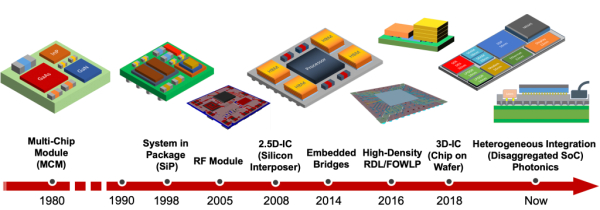
Advanced packaging technology is moving from individual IC units to integrating multiple ICs and passive components into a modular form. It is evolving from traditional lead frame-based methods such as QFN and TSOP, to BGA and FC using solder balls and bumps, and to FO-WLP and TSV, which enable the implementation of highly integrated and multi-functional semiconductors.
This is the result of a series of attempts to bridge the size gap between nanometer-level ICs and micrometer-level package substrates, such as introducing semiconductor processes to internal package interconnects or incorporating numerous external components into a single package to reduce the number of external terminals. In particular, fine interconnections between ICs utilizing the entire process minimize transmission loss and parasitic components, enabling high-speed data transmission and high-frequency operation.
◇ Next-generation packaging technologies to watch out for
FC (Flip-Chip) packaging, a conventional ball grid array (BGA) packaging technology, places the chip and substrate face-to-face, directly bonding solder bumps formed on the semiconductor chip to the substrate's wiring electrodes. Compared to wire bonding, FC packaging offers impedance less than 1/10th, allowing for package size reduction down to a single die. It also offers excellent heat dissipation.
Heterogeneous integration (HI), which has been actively utilized recently, requires advanced technologies such as SiP, WLP, and TSV, but has the advantage of being able to implement multi-functionality in a small form factor while maintaining excellent electrical and thermal performance. It has the characteristic of connecting various components such as processors, memory, sensors, optical, RF, and MEMS through a redistribution layer (RDL) process rather than soldering or wire bonding.
HI technology is broadly divided into non-TSV technologies such as FO-WLP and SiP, and TSV-based methods.
System-in-Package (SiP) is a highly integrated packaging technology that integrates multiple chips into a single package to form a system, enabling multi-functionality. Compared to system-on-chip (SoC), which integrates multiple multi-functional components into a single semiconductor, SiP reduces the need for individual block changes and reduces manufacturing process dependency, leading to a wider range of applications.
WLP (Wafer level package) is a packaging technology that improves electrical characteristics and achieves miniaturization by directly bonding the chip and board area at the wafer level without a PCB substrate.
WLP technology is divided into the FI (Fan-In) method, in which the RDL wiring is formed inside the chip, and the FO (Fan-Out) method, which uses the outer area of the chip. In particular, the FO method, which is mainly used in processes below 45 nm, has a wiring area wider than the chip, and allows for various homogeneous and heterogeneous bonds, so it has superior electrical and thermal characteristics and can be miniaturized compared to the FC and FI methods.
.jpg)
A comparison of the differences between 3D-TSV technologies [Image = Samsung Electronics]
Through-silicon via (TSV) technology miniaturizes packages by forming electrodes through via holes to stack two or more semiconductor chips. It enables stacking in three-dimensional structures, such as 2.5D and 3D, thereby improving the I/O limitations, short-circuit contact defects, and signal delays inherent in conventional wire bonding.
Within the industry, TSV technology is recognized as the only way to meet escalating technological demands, beyond simple miniaturization. Recently, interest has grown not only in vertical connections but also in horizontal connections utilizing interposers.
Accordingly, the concept of interposer is expanding from a passive interposer focused on RDL function for wiring to an active interposer that includes power sources such as DC/DC converters, power supplies, and regulators. This overcomes the low conductivity and poor heat dissipation characteristics of existing PCBs or organic substrates.
Taiwan's TSMC, the world's leading foundry, is a leader in this field. Having pioneered CoWoS (Chip-on-wafer-on-substrate) technology in 2012, TSMC recently announced its fifth-generation CoWoS technology and plans to provide services for integrating next-generation HBM3 memory into GPUs from Nvidia and AMD starting later this year.
◇ The growing importance of packaging technology
Packaging technology has emerged as a technology that overcomes the technological limitations of component integration and performance improvement due to simple miniaturization, moving beyond its traditional secondary role of circuit protection.
Packaging technology is constantly evolving, with new technologies not completely replacing existing ones. Each technology is continually evolving through the development of specific materials and processes. However, the growing importance of advanced packaging technologies is also a fact. As IDMs, foundries, and component and material suppliers increasingly participate, fierce competition is unfolding with existing OSAT companies.
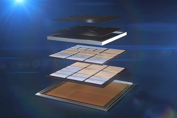
Intel unveiled its 3D stacking packaging technology, Foveros. [Capture = Intel]
Semiconductor powerhouses such as the United States, the EU, China, Taiwan, and Japan are competing to secure post-processing technologies, including packaging. Intel, renowned for its 3D packaging technology, FOVEROS, announced in 2019, plans to invest approximately 4 trillion won (approximately $3.5 billion USD) to establish a semiconductor back-end processing facility in New Mexico, USA. TSMC is establishing a packaging R&D center in Ibaraki Prefecture, Japan. Existing OSAT powerhouses such as ASE of Taiwan, Amkor of the US, and JCET of China are also actively conducting research.
Packaging technology is known to be relatively easy to enter compared to the entire process, as it is diversified by application. In June, market research firm Yole Development projected that the semiconductor advanced packaging market would grow at a CAGR of 7.6% from 2020 to 2026, reaching approximately KRW 44.7 trillion.
The entire domestic semiconductor industry is built around memory, and the post-processing industry is also memory-centric. As of 2020, three domestic companies ranked among the top 25 global OSAT companies: SFA, Hana Micron, and Nepes. Of these, SFA and Hana Micron rely heavily on outsourcing from Samsung Electronics, while Nepes is investing in FC and WLP processes.
As demand for high-performance semiconductors grows across various industries, driving the need for miniaturization and high integration, application design challenges such as electromagnetic interference (EMI) caused by unexpected electrical phenomena are emerging. Consequently, fostering related industries through the establishment of a verification infrastructure to support domestic packaging R&D and the promotion of specialized prototype production projects is urgently needed.
Comments
Related news
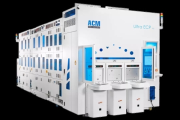
ACM Announces 'WLP Product Family' for Semiconductor Back-end Processing Companies
ACM has announced a diverse portfolio of wet wafer processing products to advance solution technology at semiconductor backend (OSAT) companies. ACM's advanced wet wafer processing products, optimized to meet customer requirements, support cutting-edge semiconductor packaging processes such as Cu pillars, Au bumping, TSV, and fan-out, and can be utilized across semiconductor processes including coating, development, plating, planarization, photoresist stripping, and etching.
2020.10.27by 강정규 기자

[China Briefing] TSMC Commercializes 5th Generation CoWoS Packaging
e4ds News - China ICT Briefing - August 24, 2021 [China Briefing]: ◇TSMC Announces New CoWoS, Preparing for Next-Generation HBM3 Products ◇BOE Secures 6th Generation Amoled AMOLED Mass Production Capability ◇Huawei Patents Message GUI Available Across Various Devices ◇Honor, Former Huawei Subsidiary, Officially Launches Magic 3 Pro, etc.
2021.08.24by 이춘영 외신
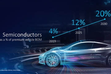
Intel to build two foundries in Europe to meet mobility demand
Pat Gelsinger, Intel CEO, forecasted that semiconductors will account for more than 20% of total premium vehicle component costs by 2030. He stated that Intel will invest up to 80 billion euros over the next decade to construct at least two fabs in Europe in response to the EU mobility industry.
2021.09.08by 이수민 기자

Intel Unveils Next-Generation 'Core Ultra Series 3' and vPro Platform for Enterprise PCs
Intel has officially unveiled the "Intel Core Ultra Series 3" for next-generation enterprise PCs and the latest vPro platform, addressing a wide range of demands from enterprise notebooks to high-performance workstations.
2026.03.26by 배종인 기자

ROHM Launches ESD Protection Diode Compatible with High-Speed Interfaces of 10Gbps or Higher
Semiconductor specialist ROHM has developed the 'RESDxVx series' of ESD (electrostatic discharge) protection diodes capable of responding to next-generation high-speed data communication environments exceeding 10Gbps, simultaneously enhancing both signal quality maintenance required in high-speed interfaces and IC protection performance.
2026.03.26by 배종인 기자











