


Samsung Electronics Ships First 3nm Semiconductor
 Published2022.07.25 10:00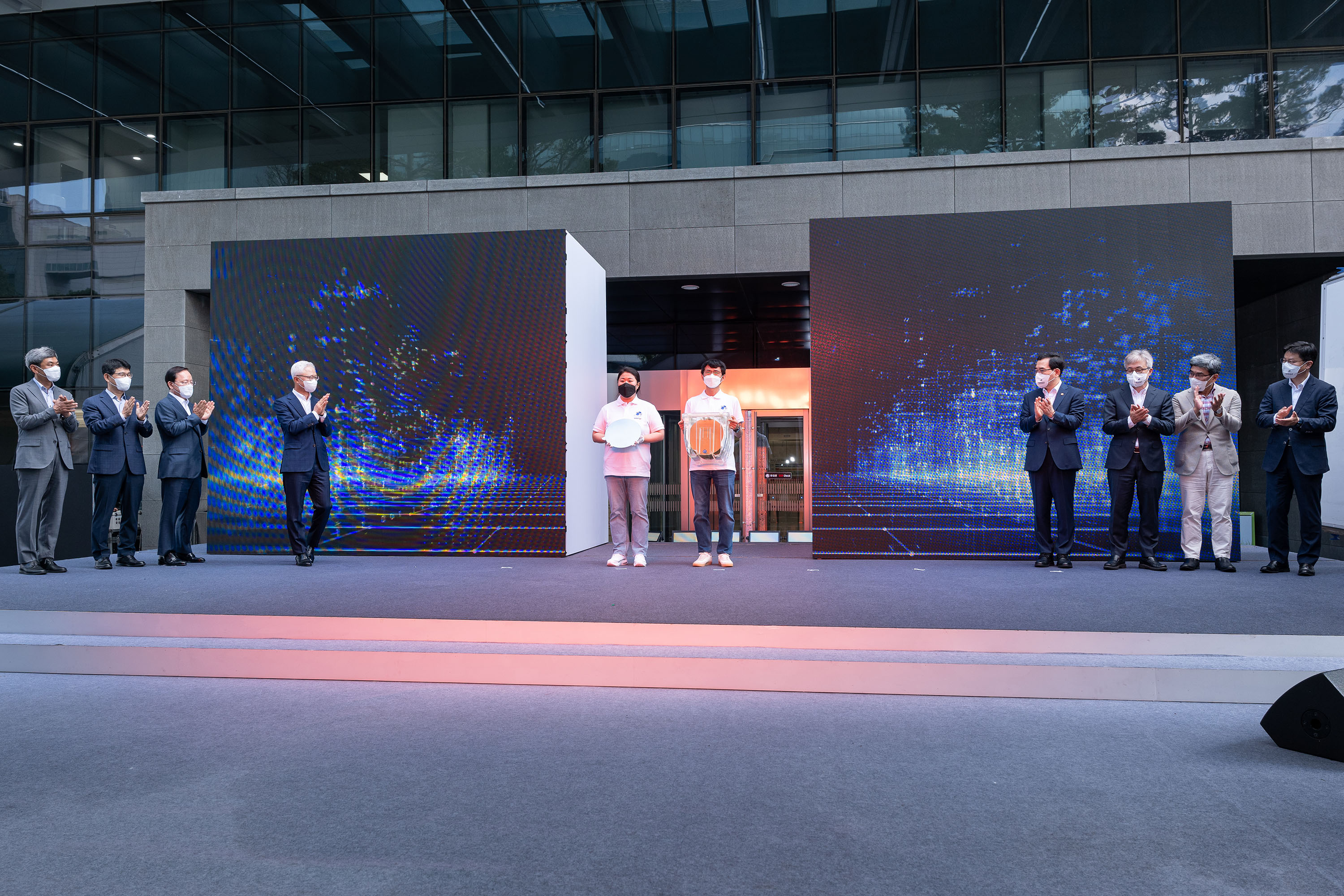
▲ Samsung Electronics World's First 3nm Foundry Shipment Ceremony (Photo - Samsung Electronics)
Hwaseong V1 Line Shipment Ceremony, Mass Production with Proprietary MBCFET Structure
Samsung Electronics, which became the first in the world to begin mass production of 3-nanometer semiconductors, held a product shipment ceremony and demonstrated its technological prowess in the global foundry market.
On the 25th, Samsung Electronics held a shipment ceremony for 3-nanometer foundry products using next-generation transistor GAA (Gate All Around) technology at the V1 line (EUV dedicated) of its Hwaseong Campus in Gyeonggi-do.
The event was attended by about 100 people, including Minister of Trade, Industry and Energy Lee Chang-yang, partners, fabless companies, and Samsung Electronics DS Division Head Kyung Kye-hyun (President) and employees, who encouraged the employees involved in the research and development and mass production of 3nm GAA.
It was reported that the representatives of affiliated companies attending the 3nm shipment ceremony included Kim Young-jae, CEO of Daeduck Electronics; Lee Jun-hyeok, CEO of Dongjin Semichem; Jung Hyeok-seok, CEO of Solbrain; Kim Chang-hyun, CEO of Wonsemicon; Lee Hyun-deok, CEO of Wonik IPS; Lee Kyung-il, CEO of PSK; Ko Sang-geol, Vice Chairman of KC Tech; and Lee Jang-gyu, CEO of Telechips.
Samsung Electronics' Foundry Business is focusing on strengthening business competitiveness through mass production of the 3nm GAA process and proactive foundry technology. Samsung announced that it has started mass production of 3nm GAA foundry process products at its Hwaseong campus and plans to expand this to its Pyeongtaek campus in the future.
Jeong Gi-tae, Vice President of Samsung Electronics’ Foundry Business, explained the process from development to mass production through a progress report on technology development, emphasizing how limitations in technology development were overcome through cross-division collaboration involving the Foundry Business, Semiconductor Research Institute, and Global Manufacturing & Infrastructure Headquarters.
Samsung Electronics DS Division President Kyung-Hyun Kye encouraged employees by saying, "Samsung Electronics has made a mark in the foundry business with the mass production of this product," and added, "The early success in developing GAA technology, which will be a new alternative when FinFET transistors reach their technological limits, is an innovative result that creates something out of nothing."
In his congratulatory remarks, Minister of Trade, Industry and Energy Lee Chang-yang expressed gratitude for the hard work of Samsung Electronics employees and the semiconductor industry, and urged Samsung Electronics, the system semiconductor industry, and the materials, parts, and equipment (Sobujang) industry to join forces to stay ahead in the fierce competition for advanced microfabrication. He emphasized that "based on the 'Strategy for Achieving Semiconductor Superpower Status' announced last week, the government will spare no effort in supporting private investment, fostering talent, developing technology, and building a Sobujang ecosystem."
Samsung Electronics began researching GAA transistor structures in the early 2000s and applied them to the 3-nanometer process in earnest starting in 2017, and last month announced the world's first mass production of the 3-nanometer process with GAA technology. It is reported that the 3nm GAA process has been applied to high-performance computing (HPC) for the first time and is being collaborated with major customers to expand its application to various product lines, including mobile SoC products.
Lee Hyun-deok, CEO of Wonik IPS, a domestic semiconductor equipment company who attended the event, stated, "As we prepare for mass production of the 3nm GAA foundry process together with Samsung Electronics, the capabilities of Wonik IPS employees have been further strengthened," adding, "We will continue to do our best together with Samsung Electronics for the development of the domestic semiconductor equipment industry."
In addition, Lee Jang-kyu, CEO of domestic fabless company Telechips, said, "Telechips has high expectations for designing future products using Samsung Electronics' ultra-fine process," adding, "Samsung Electronics is actively providing ultra-fine foundry processes to domestic fabless companies and offering various support measures to help them expand their product design scope."
Meanwhile, TSMC has announced plans for 3nm mass production in the second half of this year, and it appears that the existing FinFET process will be applied. Attention is focused on what kind of butterfly effect Samsung Electronics' preemptive introduction of the next-generation MBCFET process compared to the existing one will trigger in the future.

Comments
Related news
TSMC to begin mass production of 3nm process in the second half of 2022
TSMC announced that it will begin trial production of 4-nanometer semiconductors in the third quarter of this year, and that 3-nanometer semiconductors will enter mass production in earnest in the second half of next year.
2021.06.04by 배종인 기자
Samsung Electronics Strengthens Foundry's Cutting-Edge Process-Based Chip Implementation Solutions
Samsung Electronics is strengthening its foundry cutting-edge solutions with △3-nanometer design infrastructure △AI EDA technology △2.5D/3D packaging.
2021.11.19by 배종인 기자
Samsung's Super Gap, World's First GAA-Based 3nm Semiconductor Mass Production Begins
Ten years ago, Samsung held only about 1% of the global foundry market share, but has now narrowed the gap enough to challenge TSMC, the current foundry leader. Within five years of launching Samsung Electronics' foundry business division, the company unveiled the world's first GAA-based 3-nanometer process and is demonstrating a pace in process miniaturization that is at least one step ahead of TSMC.
2022.06.30by 명세환 기자

Intel Unveils Next-Generation 'Core Ultra Series 3' and vPro Platform for Enterprise PCs
Intel has officially unveiled the "Intel Core Ultra Series 3" for next-generation enterprise PCs and the latest vPro platform, addressing a wide range of demands from enterprise notebooks to high-performance workstations.
2026.03.26by 배종인 기자

ROHM Launches ESD Protection Diode Compatible with High-Speed Interfaces of 10Gbps or Higher
Semiconductor specialist ROHM has developed the 'RESDxVx series' of ESD (electrostatic discharge) protection diodes capable of responding to next-generation high-speed data communication environments exceeding 10Gbps, simultaneously enhancing both signal quality maintenance required in high-speed interfaces and IC protection performance.
2026.03.26by 배종인 기자











