



[SEMICON Korea 2023] “Hybrid Bonding, Hot Interest”… Global Small Business Capabilities Focused
 Published2023.02.08 12:26
Besi·EVG·AMAT, 차세대 본딩 생태계
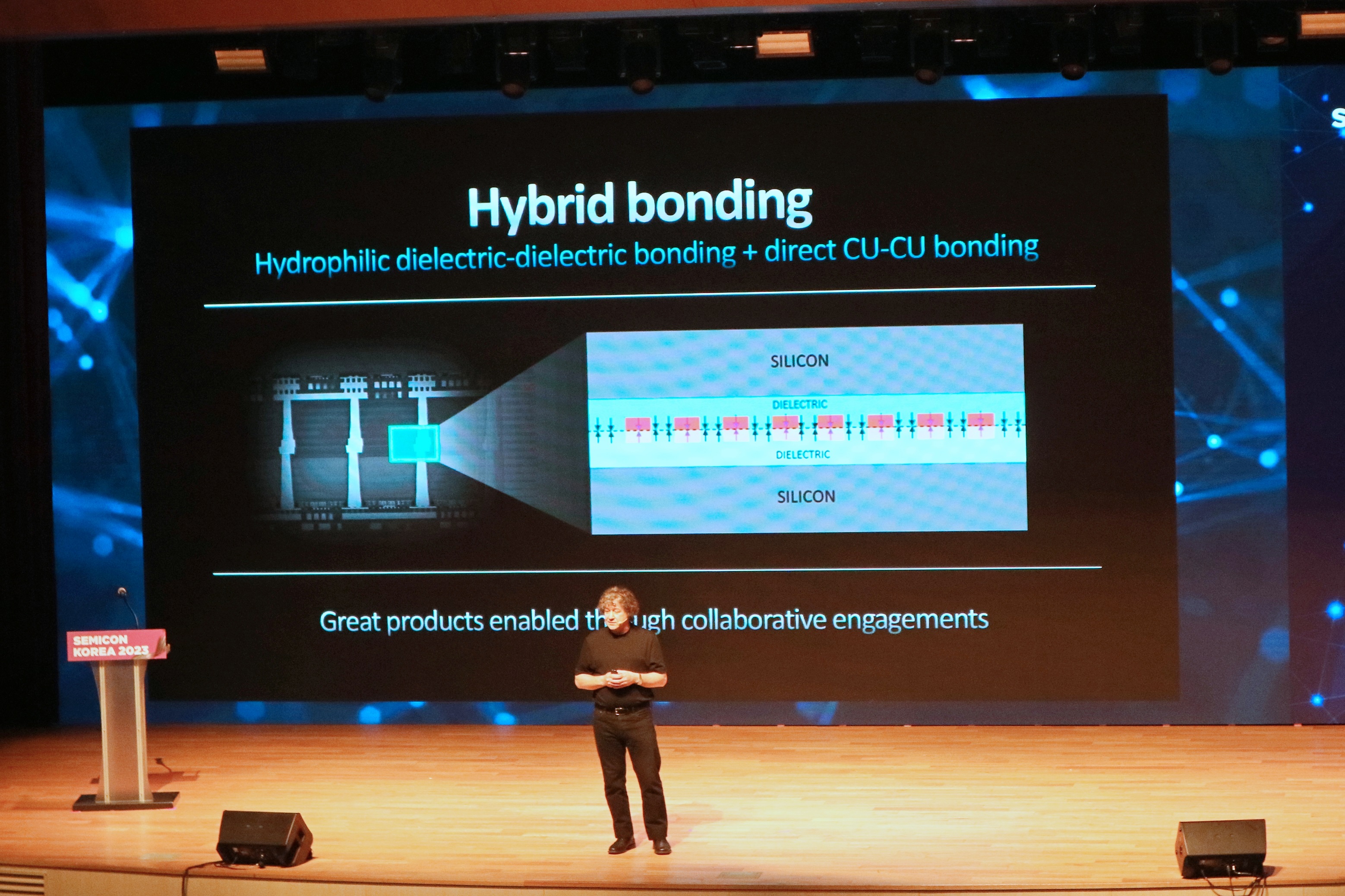
▲조셉 마크리 AMD 부사장이 세미콘 코리아 2023에서 기조연설을 진행하는 모습
“다이 투 웨이퍼 하이브리드 본딩(Die to Wafer Hybird Bonding, D2W 본딩), 이것은 오랫동안 기술 개발해왔으나 스케일링은 이제부터 시작이다”
에릭 베인 imec 부사장이 지난 세미콘 코리아 2023에서 한 말이다. 그는 D2W 하이브리드 본딩이 10µm 상호연결 피치(Interconnect Pitch) 이하에서 2µm 피치까지 상당히 유망할 것으로 내다봤다.
반도체 스케일 다운의 역사는 ‘고집적’의 역사이다. 동일 면적에 얼마나 많은 반도체 소자를 집적시키는지가 성패를 좌우했다. EUV 기술을 활용해 선폭의 미세화를 실현한 지금, 미세화의 물리적 한계는 명약관화했다.
이러한 가운데 소자의 RC 딜레이보다 BEOL(Back End of Line)공정에서 배선의 RC 딜레이가 성능 저하의 원인으로 지목받으며 패키징으로 시선이 모아지고 있다.
반도체 업계는 패키징에서 상호연결(Interconnection)의 최적화를 위해 오랫동안 고민하며 기술 발전을 도모해왔다. 오늘날 칩렛, 3D 적층 등의 구조에선 I/O를 더 많이 더 짧고 효율적으로 만들기 위한 인터커넥트 기술이 필연적으로 요구되며 관련 기술 개발이 활발한 상황이다.
■ 하이브리드 본딩, AMD-TSMC發 D2W 쇼크웨이브
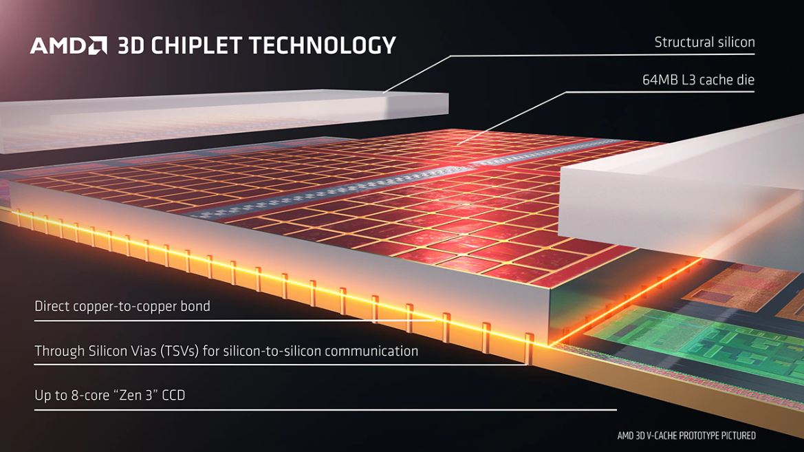
▲AMD 라이젠7 5800X3D에 적용된 3D 칩렛 기술. 3D V-Cache는 구리 하이브리드 본딩을 통해 D2W를 실현했다.(이미지-AMD)

최근 뜨거운 시선이 모아지고 있는 하이브리드 본딩은 마이크로범프의 피치 한계에 따라 차세대 기술로 떠올랐다. 이미 CMOS 이미지 센서에서 웨이퍼 투 웨이퍼(Wafer to Wafer, W2W) 하이브리드 본딩이 대량 생산에 적용된 가운데 기술 성숙도가 떨어져 실제품에 적용되지 않던 D2W 기술이 AMD 제품에서 적용됐다.
AMD는 지난 2022년 4월 라이젠7 5800X3D를 출시했다. 수년간 개발한 AMD의 3D V-Cache는 구리 하이브리드 본딩을 통해 D2W를 실현한 기술이며 이것이 적용된 첫 제품이 바로 라이젠7 5800X3D이다. 기존 32MB L3 캐시에 64MB 캐시 다이를 쌓아 올려 총 96MB L3 캐시를 구현했다.
다이와 웨이퍼 간 구리 결선을 통해 I/O 밀도를 높이고 배선 길이를 줄여 성능·전력효율 등 전반에서 스케일 다운을 이뤘다.
조셉 마크리 AMD 부사장은 3D V-Cache가 상호연결 밀도(Interconnect Density) 면에서 △2D 칩렛에 200배 △3D 패키징에서 마이크로 범프 대비 15배 더 고집적해 있으며, 에너지 효율성은 3배가량 더 높아진다고 설명했다.
TSMC의 7나노 공정을 기반으로 3D SoIC 기술이 적용됐으며 다가올 2월에 출시될 라이젠9 7950X3D는 TSMC 5나노 핀펫 공정에서 양산되며 128MB L3 캐시를 적층했다. AMD는 3D 아키텍처에서 하이브리드 본딩을 통해 9µm 피치를 달성할 수 있다고 전했다. 현재 세대인 Zen3 아키텍처에서는 TSV 피치가 17µm인 것으로 알려진 가운데 차세대 아키텍처인 Zen4에서는 이 피치가 더 줄어들 것으로 전망된다.
imec 에릭 베인 부사장은 “D2W에서 다이렉트 방식은 파티클에 의한 디펙트 위험이 크기에 콜렉티브 방식(Collective D2W)을 통해 파티클 문제를 해결할 것”을 언급했다.
다이렉트 방식은 다이 배치 중 파티클 관리에 어려움이 있는 반면 콜렉티브 방식은 검증된 기술로 W2W 하이브리드 본딩과 동등한 다이 활성화 및 세정에 장점이 있으며, 산화물 관리와 캐리어 상에서 재작업이 가능한 것이 이점으로 꼽힌다. 다만 캐리어 준비 및 세정 등에서 추가적인 비용이 발생할 수 있다.
.jpg)
▲imec 에릭 베인 부사장이 세미콘 코리아 2023서 W2W, D2W 등 3D 인터커넥트 로드맵을 발표하고 있다.
■ Besi·EVG·AMAT, 하이브리드 생태계 구축
차세대 패키징 시장에서 하이브리드 본딩 솔루션을 두고 장비사들의 움직임이 분주하다. 업계는 새로운 성장 기회를 잡고자 생태계 조성과 협력을 통한 로드맵 가속화도 마다하지 않는 모습이었다.
.jpg)
▲세미콘 코리아 2023서 분비는 Besi 부스의 모습
Besi는 △다이 어태치(Die Attach) △패키징 △플레이팅(Plating)에서 포트폴리오를 가지고 있으며 △다이 본딩 △다중 모듈 부착 △소프트 솔더 다이 본딩 △플립 칩 등에서 장비를 개발·생산하고 있다.
EV그룹(EVG)은 △반도체 △MEMS △화합물 반도체 △파워 디바이스에 필요한 장비와 공정 솔루션을 제공하는 기업으로 나노기술을 이용한 소자 개발에 필요한 기술력을 갖추고 있다. EVG는 △D2W를 비롯한 본딩 △리소그래피 △계측 시스템 등의 제품군을 보유하고 있으며, △하이브리드 본딩 △Eutectic wafer bonding △Com bond 기술 등 다양한 본딩 기술을 갖추고 있다.
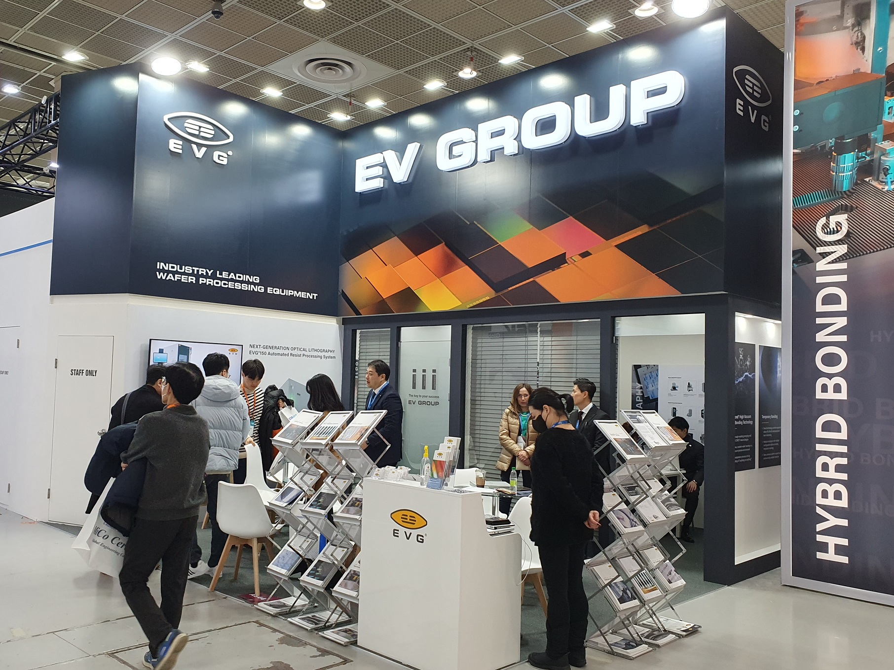
▲세미콘 코리아 2023서 하이브리드 본딩 솔루션을 적극 과시하는 EVG
EVG도 AMAT와 손을 잡고 W2W 하이브리드 본딩의 공동 개발을 진행하고 있다. 토마스 어만 EVG 사업개발 디렉터는 “반도체 혁신에서 3D 접합 및 공학재료의 중요도는 갈수록 증가하고 있으며 이에 따른 하이브리드 웨이퍼 본딩 수요도 매우 높다”고 말한 바 있다.
빈센트 디카프리오 AMAT 첨단 패키징 사업개발 부문 매니징 디렉터는 “반도체 제조사가 이종 설계 비중을 높이는 가운데 어플라이드는 Besi, EVG와 같은 파트너와 협업해 D2W, W2W를 포함한 하이브리드 본딩 기술 개발과 도입에 필요한 역량을 제공하고 있다”고 밝혔다.

Comments
Related news
.jpg)
[Korean Institute of Electromagnetic Engineering & Construction Summer Conference] Future of 2.5 and 3D Semiconductors, “Power and Signal Integrity Essential”
While the global population is approximately 7.7 billion, the number of devices in use exceeds 500 billion. Unlike the 2000s when PC and mobile phone penetration rates per capita were minimal, semiconductor trends have shifted significantly. According to Cisco's Global Cloud Index data, from 2008 onward, the number of devices surpassed the population count, with an average of 15 devices per person. Projections now anticipate 1.25 trillion devices by 2030.
2022.08.25by 명세환 기자

Intel Unveils Next-Generation 'Core Ultra Series 3' and vPro Platform for Enterprise PCs
Intel has officially unveiled the "Intel Core Ultra Series 3" for next-generation enterprise PCs and the latest vPro platform, addressing a wide range of demands from enterprise notebooks to high-performance workstations.
2026.03.26by 배종인 기자

ROHM Launches ESD Protection Diode Compatible with High-Speed Interfaces of 10Gbps or Higher
Semiconductor specialist ROHM has developed the 'RESDxVx series' of ESD (electrostatic discharge) protection diodes capable of responding to next-generation high-speed data communication environments exceeding 10Gbps, simultaneously enhancing both signal quality maintenance required in high-speed interfaces and IC protection performance.
2026.03.26by 배종인 기자

ST Launches 75V Drive IC Targeting 48V Industrial Motor Driving
ST Microelectronics has unveiled the 'STSPIN9P' series of 75V motor drive ICs tailored for 48V-class industrial drive system design. The new product family is characterized by half-bridge and full-bridge configurations that enable design scalability according to motor type and output conditions. Power supply circuits, protection functions, and current sensing circuits are integrated on-chip to simplify system configuration, and the devices are designed to support applications up to 500W maximum. The company plans to provide reference designs and demo boards to support development and evaluation in industrial automation, robotics, pumps, fans, lighting, and textile machinery.
2026.03.26by 배종인 기자

Nordic supports security updates for the entire lifecycle of IoT devices at a single fixed cost
Nordic Semiconductor, a global leader in low-power wireless connectivity solutions, has unveiled a single fixed-cost licensing model that delivers FOTA (Firmware Over-the-Air) and device management capabilities throughout the device lifecycle via nRF Cloud, and introduced a new firmware update solution to prepare for the enforcement of the European Union's Cyber Resilience Act (CRA).
2026.03.26by 배종인 기자











