



Semiconductor Packaging Materials Market to be Worth $30 Billion by 2027
 Published2023.05.24 15:39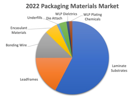
The global semiconductor packaging materials market is expected to grow at a CAGR of 2.7% to reach approximately USD 30 billion by 2027, driven by increasing demand for advanced packaging solutions.
SEMI, an industry association representing the global electronics industry supply chain, forecasted that the global semiconductor packaging materials market will grow at a CAGR of 2.7% from $26.1 billion in 2022 to $29.8 billion in 2027 due to technological innovation and increasing demand for advanced electronic products.
This outlook is based on the Global Semiconductor Packaging Materials Outlook report jointly produced by SEMI, TECHCET and TechSearch.
This growth is expected to be driven by increasing demand for advanced packaging solutions driven by the adoption of high-performance applications, 5G, artificial intelligence (AI), heterogeneous integration, and system-in-package technologies.
“The semiconductor packaging materials industry is undergoing significant change as new technologies and applications drive increased demand for a wider range of materials,” said Jan Baderman, CEO of TechSearch. “Advances in dielectric materials and underfill materials are driving the demand for fan-in and fan-out wafer-level packaging, flip-chip, and 2.5D/3D packaging. New substrate technologies such as silicon interposers and organic interposers using RDL (Re-Distribution Layer) are also emerging as major growth drivers for packaging solutions. In addition, research on glass core substrates and laminate substrates with finer properties is also ongoing,” he said.
The Global Semiconductor Packaging Materials Outlook (GSPMO) report cited in this announcement provides a comprehensive analysis of the current and projected semiconductor packaging materials, including substrates, leadframes, bonding wires, encapsulation materials, underfill materials, die attach, wafer-level package dielectrics, and wafer-level plating chemicals.
Meanwhile, e4ds will host the ' 2023 e4ds Semiconductor Packaging Day ' event at the Korea Conference Center Main Hall on June 28. At this seminar, top domestic and international packaging experts, including Intel, Nepes, Applied Materials, Hanyang University, and Hyundai Motor Securities, will present on next-generation packaging solutions. Participation in the event can be done on the ' 2023 e4ds Semiconductor Packaging Day ' ( https://www.e4ds.com/seminar_introduce.asp?idx=137 ) website.

Comments
Related news

Intel Unveils Next-Generation 'Core Ultra Series 3' and vPro Platform for Enterprise PCs
Intel has officially unveiled the "Intel Core Ultra Series 3" for next-generation enterprise PCs and the latest vPro platform, addressing a wide range of demands from enterprise notebooks to high-performance workstations.
2026.03.26by 배종인 기자

ROHM Launches ESD Protection Diode Compatible with High-Speed Interfaces of 10Gbps or Higher
Semiconductor specialist ROHM has developed the 'RESDxVx series' of ESD (electrostatic discharge) protection diodes capable of responding to next-generation high-speed data communication environments exceeding 10Gbps, simultaneously enhancing both signal quality maintenance required in high-speed interfaces and IC protection performance.
2026.03.26by 배종인 기자

ST Launches 75V Drive IC Targeting 48V Industrial Motor Driving
ST Microelectronics has unveiled the 'STSPIN9P' series of 75V motor drive ICs tailored for 48V-class industrial drive system design. The new product family is characterized by half-bridge and full-bridge configurations that enable design scalability according to motor type and output conditions. Power supply circuits, protection functions, and current sensing circuits are integrated on-chip to simplify system configuration, and the devices are designed to support applications up to 500W maximum. The company plans to provide reference designs and demo boards to support development and evaluation in industrial automation, robotics, pumps, fans, lighting, and textile machinery.
2026.03.26by 배종인 기자

Nordic supports security updates for the entire lifecycle of IoT devices at a single fixed cost
Nordic Semiconductor, a global leader in low-power wireless connectivity solutions, has unveiled a single fixed-cost licensing model that delivers FOTA (Firmware Over-the-Air) and device management capabilities throughout the device lifecycle via nRF Cloud, and introduced a new firmware update solution to prepare for the enforcement of the European Union's Cyber Resilience Act (CRA).
2026.03.26by 배종인 기자
Schneider Aims for Building Energy Savings and Operational Stability with Next-Generation HVAC Drives
Schneider Electric has unveiled its next-generation HVAC drive product line 'Altivar HVAC'. The new product line's key features center on enhanced energy savings, system operational stability, and building management system integration. The products are divided into 'ATH200' for OEM and small equipment applications, and 'ATH600' for environments requiring continuous operation and advanced control. The company plans to expand the application scope from commercial buildings to facilities where HVAC system stability is critical, such as hospitals, airports, and data centers. The announcement includes over 30% energy savings, operation from -10°C to +60°C, Modbus and BACnet support, and compatibility with low global warming potential refrigerants.
2026.03.26by 명세환 기자











