


Cadence Supports Samsung Foundry's Development of Advanced Packaging Technology
 Published2023.07.06 09:30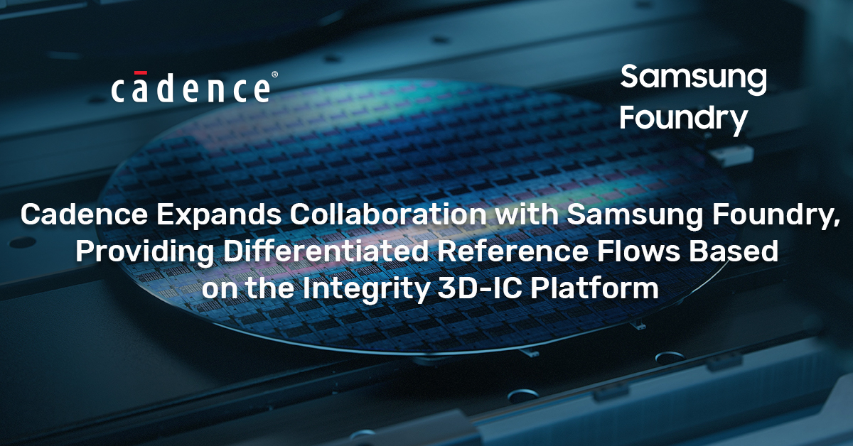
▲Cadence collaborates with Samsung Foundry (Image: Cadence)
Support for multi-die chip implementation and advanced packaging development
As interest in and demand for advanced packaging for heterogeneous integration grows, global semiconductor design automation company Cadence and Samsung Electronics, a leading Korean foundry, have joined forces to accelerate 3D-IC design development.
Cadence Design Systems, Inc. announced today that it has expanded its collaboration with Samsung Foundry to accelerate the development of 3D-IC designs for next-generation applications such as hyperscale computing, 5G, artificial intelligence (AI), the Internet of Things (IoT), and mobile.
This collaboration is expected to accelerate multi-die chip development by providing the latest reference flow and related package design kit. It is based on Cadence Integrity 3D-IC, the industry’s only integrated platform, providing system planning, packaging, and system-level analysis in a single cockpit.
Cadence Integrity 3D-IC platform supports Samsung's new 3D CODE standard. This standard is a new system description language that simplifies the definition and interoperability of design generation and analysis flows in an integrated environment.
When designing advanced package multi-die chips, engineers can face the following challenges: △Design analysis and flow complexity, △Configuration challenges, and △System-level thermal and power integrity issues. All of these issues can increase design time. To address these challenges, integrated, comprehensive solutions such as △Reference Flow, △Package Design Kit, and △Samsung’s 3D CODE standard can simplify the multi-die chip design and implementation process, increasing productivity and reducing design iteration times.
Based on the 'Cadence Integrity 3D-IC' platform, the reference flow provides key capabilities such as early analysis for Power Delivery Network (PDN), Layout Versus Schematic (LVS), and Design Rule Checking (DRC). These flows also provide additional productivity benefits by integrating Cadence Allegro X packaging technology with multiphysics system-level analysis tools, Celsius Thermal Solver and Clarity 3D Solver.
“We aim to provide customers designing high-performance products with the benefits of advanced packaging technologies such as lower power, lower yield cost and improved system performance,” said Kim Sang-yoon, senior vice president of Foundry Business at Samsung Electronics. “With the introduction of our 3D CODE technology and Cadence’s comprehensive new flow, we are supporting our mutual customers in achieving their multi-die chip implementation goals and delivering the next-generation chip architectures they need to quickly bring high-quality products to market.”
“Cadence’s ongoing collaboration with Samsung Foundry helps customers achieve a competitive advantage with our multi-die chip design platform,” said Vivek Mishra, vice president of Cadence Digital and Signoff Group. “Combining reference flows based on our Cadence Integrity 3D-IC platform with Samsung’s latest technologies provides customers with a unified design environment that streamlines their workflow when creating complex 3D-IC designs and reduces the time required to implement multi-die chips.”

Comments
Related news
“Advanced Packaging, Transformation of Technology-Intensive Industry”
As advanced packaging technology becomes increasingly important for implementing advanced semiconductors, an event where visitors could explore the latest surface mounting technology and packaging-related technology trends was held in one venue, drawing continued foot traffic from attendees.
2023.04.05by 명세환 기자

Cadence Provides Fast Path to Mobile Chip Tapeout Using ARM TCS23
Cadence Design Systems (hereinafter Cadence) announced on the 13th that it will strengthen its ongoing collaboration with ARM for successful tapeout of mobile device silicon by providing customers with a tapeout pathway using digital verification tools and ARM's recently launched Total Compute Solution (TCS23), enabling them to complete chip design and move into the manufacturing preparation stage.
2023.06.14by 명세환 기자
Semiconductor Market Recovery Remains Question Mark This Year… Focus on AI Semiconductors
At the 2023 e4ds Semiconductor Packaging Day, there were forecasts suggesting that the semiconductor market this year may not recover easily.
2023.07.03by 명세환 기자

Intel Unveils Next-Generation 'Core Ultra Series 3' and vPro Platform for Enterprise PCs
Intel has officially unveiled the "Intel Core Ultra Series 3" for next-generation enterprise PCs and the latest vPro platform, addressing a wide range of demands from enterprise notebooks to high-performance workstations.
2026.03.26by 배종인 기자

ROHM Launches ESD Protection Diode Compatible with High-Speed Interfaces of 10Gbps or Higher
Semiconductor specialist ROHM has developed the 'RESDxVx series' of ESD (electrostatic discharge) protection diodes capable of responding to next-generation high-speed data communication environments exceeding 10Gbps, simultaneously enhancing both signal quality maintenance required in high-speed interfaces and IC protection performance.
2026.03.26by 배종인 기자











