


Intel Foundry Builds High NA EUV
 Published2024.04.19 12:17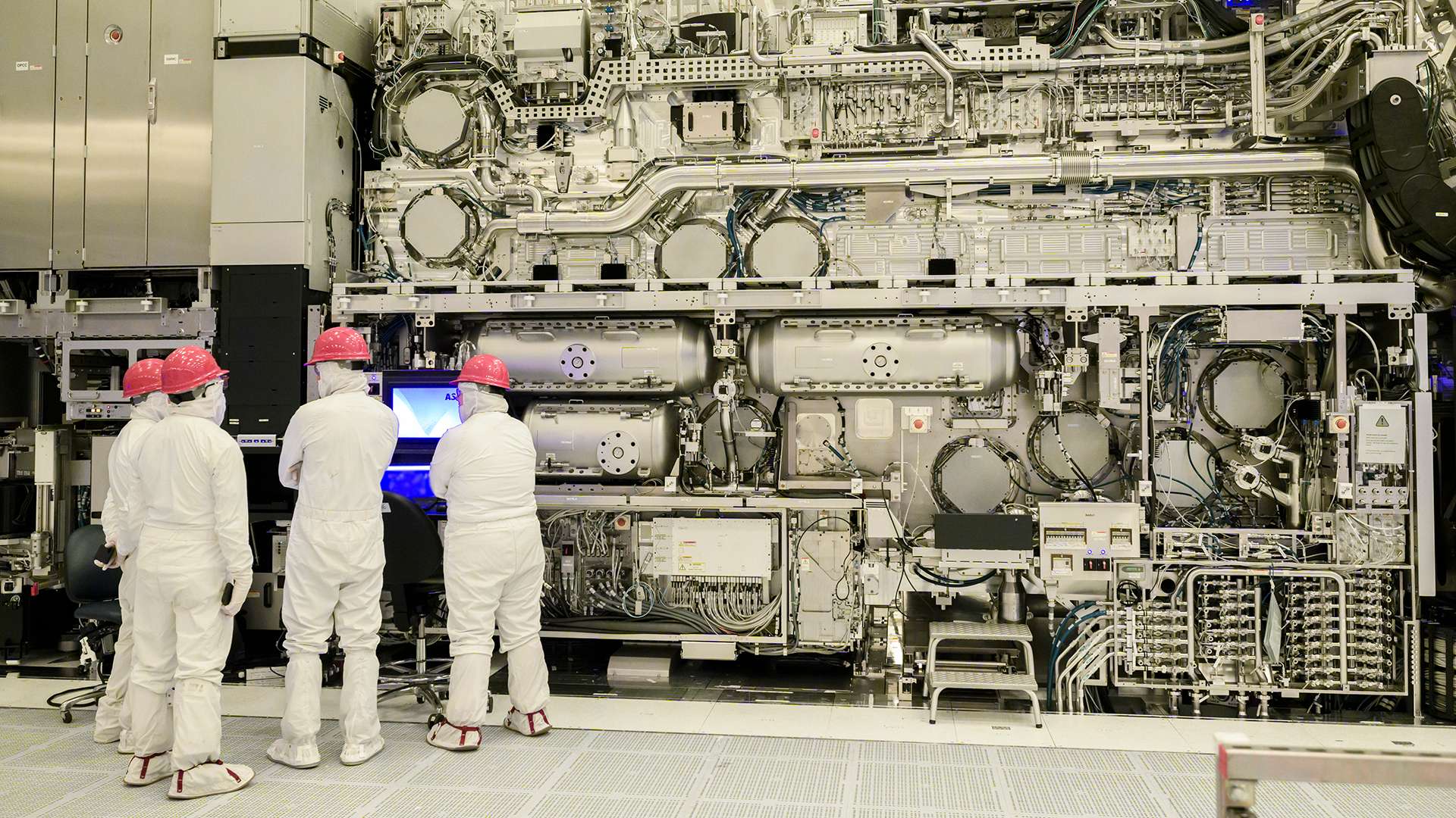
▲ Intel Foundry leads chip manufacturing with the introduction of High-NA Extreme Ultraviolet (High-NA) lithography (Photo: Intel)
Intel, which is building NA EUV lithography equipment in its foundry, stands at the forefront of the expansion of Moore's Law and is accelerating the transition to the Angstrom Era.
Intel Foundry announced on the 19th that it has completed the assembly of the industry's first High NA EUV lithography equipment located in the Hillsboro R&D area in Oregon.
It has been reported that ASML’s High NA EUV equipment, the TwinScan EXE:5000, is undergoing several calibration stages to be prepared for use in Intel’s advanced process roadmap development.
The latest EUV equipment is known to be capable of dramatically improving the resolution and functionality of next-generation processors through changes in optical design for projecting printed images onto silicon wafers.
Mark Phillips, Intel’s Director, stated, “With the addition of High NA EUV, Intel now possesses the most versatile lithography equipment in the industry and has the capability to drive future processes beyond Intel 18A after 2025.”
Intel Foundry runs at full specifications As a preliminary step, the equipment's optical devices, sensors, and stage were roughly calibrated and then the image was transferred. ASML technology, capable of printing circuits with 10 nm integration using a full-field optical exposure system, is a key element for the commercialization of high NA EUV equipment.
High NA EUV is expected to be able to transfer up to 1.7 times finer than existing EUV equipment, enabling the expansion of 2D capabilities and improving integration density by 2.9 times. Intel is focusing its capabilities on patterning chips that are finer and more integrated.
Compared to 0.33NA EUV, High NA EUV (or 0.55NA EUV) provides higher imaging contrast with less light per exposure for similar functions, reducing the time required to print each layer. A reduction in printing time means higher wafer production volume for the fab.
Intel is expected to use both 0.33NA EUV and 0.55NA EUV along with other lithography processes when developing and manufacturing advanced chips, starting with Intel 18A product verification in 2025 and leading up to Intel 14A production.
Creating ultrafine transistors requires new transistor structures and improvements to other process steps. Intel stated that it is improving other process steps currently under development in parallel with the integration of the first High NA EUV system.
The Intel Foundry Oregon R&D site is a core department for Intel's technology and R&D, and to introduce this latest generation of lithography equipment, Intel invested more than $3 billion to expand the D1X fab in Oregon, adding 270,000 square feet of cleanroom space and opening Mod 3 in 2022.
Comments
Related news

Intel: "AI-accelerated PC supply will be a priority, with 100 million units to be delivered by next year."
Intel stated that AI represents a new opportunity for the PC industry, and that devices must be supplied in large quantities as a priority for AI advancement. The company announced that it will make every effort to ensure sufficient product supply to deliver approximately 100 million devices by next year.
2024.02.19by 배종인 기자

Intel Unveils Edge Platform, Simplifying On-Device AI Development
Competition among companies is intensifying to expand AI at the edge device layer that interfaces with consumers and end users. In this context, Intel has newly introduced an open software platform that facilitates the development, deployment, and execution of edge AI solutions for developers, operators, and enterprises.
2024.02.27by 명세환 기자
Applied Leads in Angstrom Patterning Technology
Recently, advanced semiconductor foundry processes have announced next-generation technology roadmaps for 1-2 nanometer nodes, opening the angstrom era in ultra-fine patterning. As Intel has begun earnestly implementing its 18 angstrom-based roadmap, which corresponds to 1.8 nanometers, materials and equipment suppliers are rapidly overcoming technical limitations through innovation to support these advancements.
2024.04.04by 배종인 기자
.jpg)
Intel Vision Book Gaudi 3 Unveiled... Focusing on AI Open Ecosystem
"Current AI platforms cannot meet everything. They are not open ecosystems and are locked into specific companies." Intel announced new customers and partners at Vision 2024 and unveiled an AI strategy aimed at open systems across AI. To this end, the company introduced its next-generation Gaudi3 AI accelerator, emphasizing performance comparable to NVIDIA's H200 and a comprehensive enterprise AI strategy.
2024.04.11by 권신혁 기자

Intel's World's Largest Neuromorphic System Equipped with Owl Brain-Level Neuron Capacity
Intel has unveiled the world's largest neuromorphic system with neuron capacity at the level of an owl brain, and expectations are gathering that it will help support artificial intelligence research that mimics future brain architecture and address challenges related to AI efficiency and sustainability.
2024.04.18by 배종인 기자











