



SK Hynix Vice President Lee Kang-wook Receives IEEE Electronics Packaging Society Award
 Published2024.05.31 14:20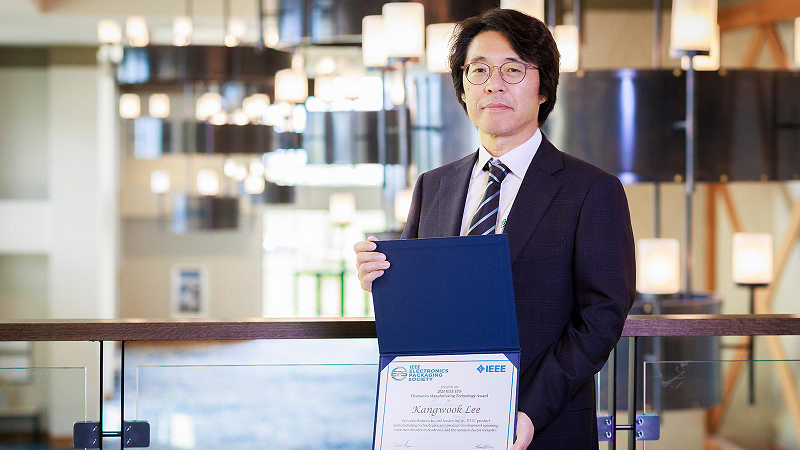
▲ Lee Kang-wook, Vice President of Package Development at SK Hynix / (Photo: SK Hynix)
The Institute of Electrical and Electronics Engineers (IEEE), the most prestigious international organization in electrical and electronic engineering, has awarded a first-ever Korean an Electronics Manufacturing Technology Award. Innovations in HBM and MR-MUF packaging are said to have contributed to this award.
SK Hynix announced on the 31st that Lee Kang-wook, Vice President of PKG Development, became the first Korean to receive the 'Electronics Manufacturing Technology Award' at the 'Institute of Electrical and Electronics Engineers (IEEE) Electronics Packaging Society (EPS) Awards 2024' held in Denver, Colorado on the 30th (US time).
This awards ceremony is an annual event hosted by the Electronics Packaging Society (EPS), a subsidiary of the Institute of Electrical and Electronics Engineers (IEEE), the most authoritative organization in the international electrical and electronic engineering field. The Electronics Manufacturing Technology Award is given to those who have made outstanding achievements in the field of electronics and semiconductor packaging. Since the first winner was announced in 1996, Vice President Lee Kang-wook has become the first Korean to be selected as the winner this year.
The Electronic Packaging Society (EPS) stated that the reason for selecting this vice president was his significant contributions to the development and advancement of AI memory, HBM, and manufacturing technology while conducting research and development in the field of 3D packaging and integrated circuits in global academia and industry for over 20 years.
This vice president, an expert in semiconductor packaging technology, received his doctorate in 'Three-dimensional Integration Technology for Integrated Micro-System' from Tohoku University in Japan in 2000. After working as a postdoctoral researcher at Rensselaer Polytechnic Institute in the United States and a professor at Tohoku University in Japan, he has been leading the development of packaging technology required for HBM products as a WLP (Wafer Level Package) developer at SK Hynix since 2018.
In particular, this vice president successfully introduced the MR-MUF (Mass Reflow Molded Underfill) packaging innovation technology during the development of HBM2E, the third-generation HBM product in 2019, playing a key role in helping SK hynix secure a dominant position in the HBM market and leap forward as a global AI memory leader.
MR-MUF is a process technology that injects and hardens a liquid-type protective material into the space between chips to protect the circuits between chips after stacking semiconductor chips. It is a more efficient technology than the method of laying down film-type material each time a chip is stacked, and is also effective in dissipating heat.
“I am very pleased that this award officially recognizes SK Hynix’s outstanding achievements in the HBM field,” said the vice president. “As the AI era begins in earnest, the role of packaging is becoming more important, so we will continue to do our best to achieve technological innovation.”rdquo; said.

Comments
Related news
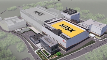
SK Hynix decides on new DRAM production base for M15X in Cheongju
SK Hynix has decided to proactively respond to the surging demand for AI semiconductors by expanding production capacity for next-generation DRAM, including HBM, which is a key component of AI infrastructure.
2024.04.25by 배종인 기자
SK Hynix CEO Kwak No-jeong: “Next year’s production of HBM also sold out”
SK Hynix CEO Kwak Noh-jung stated in a press briefing, "From a production perspective, SK Hynix HBM is already sold out this year, and next year is almost sold out as well." He added, "In terms of HBM technology, to further solidify our market leadership, we are preparing to provide samples of the world's highest-performance HBM3E 12-stack product in May, with mass production targeted for the third quarter."
2024.05.02by 배종인 기자
SK Hynix Develops Next-Generation Mobile NAND Solution 'ZUFS 4.0'
As data movement and capacity increase in the AI era, memory performance is also becoming an important factor for realizing on-device AI. SK Hynix has demonstrated next-generation technology leadership in NAND flash and achieved new milestones.
2024.05.09by 명세환 기자

SK Hynix: "We actively welcome support for the semiconductor industry."
SK Hynix expressed its active welcome for the semiconductor industry support policy announced by the government on the 23rd.
2024.05.23by 배종인 기자
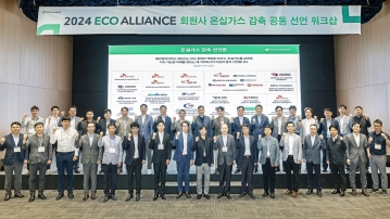
SK Hynix Strengthens Scope 3 Emissions Reductions
SK Hynix is launching full-scale efforts to reduce Scope 3 emissions—those generated outside business facilities—through the "ECO Alliance Workshop," where the company makes a joint declaration on greenhouse gas reduction with its small and medium-sized suppliers.
2024.05.29by 배종인 기자











