



KIMS Hosts Advanced Semiconductor Packaging Materials Innovation Forum… Discusses Technological Self-Reliance
 Published2026.03.16 09:46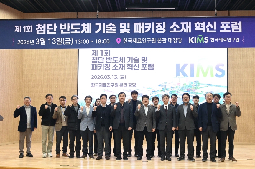
Experts from industry, academia, research institutes, and government gather in one place… Sharing trends in advanced packaging technologies such as heterogeneous integration and wiring materials
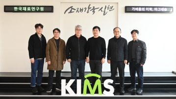
The Korea Institute of Materials Science and Engineering (KIMS) held the "1st Advanced Semiconductor Technology and Packaging Materials Innovation Forum" on March 13 at the main auditorium of its headquarters in Changwon, Gyeongnam, to discuss the future direction of advanced semiconductor packaging technology and related materials industries. The event was organized to share the current status of research and development in the field of advanced packaging, which is attracting attention as a key technology to complement the limitations of semiconductor microfabrication, and to explore cooperative frameworks.
At the event, experts from industry, academia, research institutes, and government participated in presentations and discussions centered on key issues in the semiconductor technology and materials industries. The first session covered key topics such as the development of semiconductor technology for future mobility, the characteristics of SiC power semiconductor materials, the direction of the semiconductor materials, parts, and equipment specialized complex, an advanced packaging testbed platform, and a heterogeneous integration platform for next-generation AI accelerators.
In the subsequent second session, composite semiconductor technology for smart heterogeneous integrated systems, advanced packaging wiring material technology, and research cases regarding thermal management and reliability assurance in semiconductor packaging were introduced. Following the presentations, an expert panel discussion was held on the topic of advancements in semiconductor packaging material technology, during which opinions were presented regarding directions for technological development and collaboration strategies.
Choi Chul-jin, President of the Korea Institute of Materials Science (KIMS), stated that the institute intends to strengthen its role in securing semiconductor packaging material technology as a specialized research institution in the field of materials. He expressed his hope that the forum would share an understanding of advanced packaging material technology and contribute to the formation of a cooperative network among industry, academia, and the government.

Comments
Related news
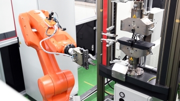
KIMS Unveils AI Autonomous Experiment Platform 'Autonomous Lab'
The Korea Institute of Materials Science (KIMS) has unveiled an "Autonomous Lab," an AI-based automated research system for the entire lifecycle. It dramatically shortens material experiment cycles that previously took several months to years, and launches full-scale efforts in material self-sufficiency and digital R&D innovation through collaboration between AI and robots.
2025.06.27by 명세환 기자
.jpg)
Korea Institute of Materials Science (KIMS) breaks new ground in unmanned aerial vehicle technology... Fuel cell drone achieves 12-hour continuous flight.
The Korea Institute of Materials Science (KIMS) has independently developed a 1.2kW-class fuel cell and succeeded in continuous flight of an unmanned aircraft utilizing this technology for over 12 hours. This achievement is evaluated as the longest domestic flight record among fuel cell-based unmanned aircraft and represents world-class technology by civilian standards.
2025.08.04by 명세환 기자
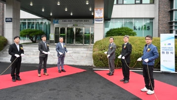
Korea Materials Research Institute Accelerates Global Collaboration in Materials Science
The Korea Institute of Materials Science (KIMS, Director Chol-Jin Choi) has established the KIMS-NIMS International Joint Research Center together with Japan's National Institute for Materials Science (NIMS, Director Kazuhiro Hono), and will conduct joint research projects at a world-class level.
2025.10.15by 명세환 기자
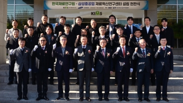
Korea Institute of Materials Science and Samsung Heavy Industries Join Forces to Secure Sovereignty in Materials
The Korea Institute of Materials Science (KIMS, Director Choi Chul-jin) and Samsung Heavy Industries (SHI) have joined forces to establish the 'KIMS-SHI Materials Innovation Research Center,' holding a dedication ceremony at the KIMS headquarters in Changwon, Gyeongnam on November 28th.
2025.12.01by 배종인 기자
The Korea Institute of Materials Science selected five projects, the largest number ever, for its 2025 National R&D Excellence List.
The Korea Institute of Materials Science (KIMS, Director Choi Cheol-jin) has raised expectations for technology transfer and commercialization as a record five projects have been selected for the 2025 National Research and Development Excellence Awards.
2025.12.24by 배종인 기자











