



Zeiss, “German Technology at Korean Speed”… Opens First Global Semiconductor Innovation Center in Yongin
 Published2026.07.10 14:54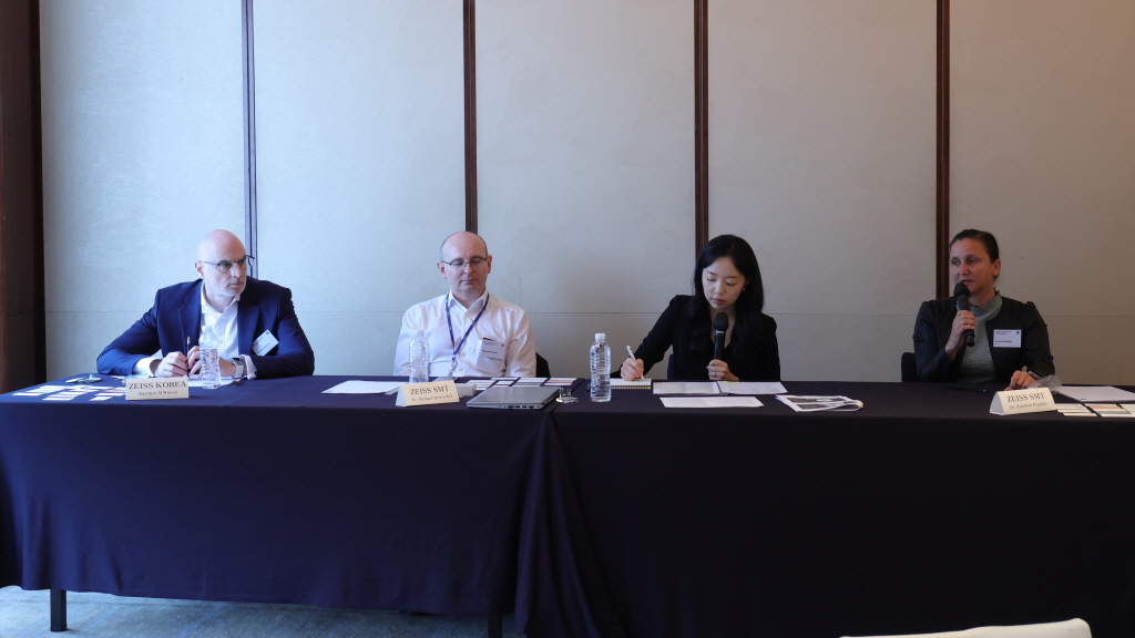
▲(왼쪽부터)매튜 윌슨 자이스코리아 부사장, 마하엘 헨첼 박사, (맨 오른쪽)카롤리네 피그돈 박사가 기자들의 질문에 답하고 있다.
결함 정보 바탕 공정 파라미터 조정 장기적 수율 개선 기여

글로벌 광학솔루션 기업 자이스가 한국 반도체 고객사와의 기술 협력을 강화하기 위해 경기도 용인에 첫 글로벌 반도체 이노베이션 센터를 열었다.
자이스(ZEISS)는 10일 기자간담회를 갖고, 경기도 용인 서플러스글로벌 반도체 장비 클러스터 내에 ‘자이스 반도체 이노베이션 센터’(ZSKIC)를 개소했다고 밝혔다.
이번 반도체 이노베이션 센터 개소를 통해 한국 고객사의 양산 공정과 첨단 패키징 기술 개발을 현장에서 지원하겠다고 밝혔다.
이번 센터는 자이스 반도체사업부가 전 세계에 처음으로 마련한 글로벌 반도체 이노베이션 센터다.
자이스는 한국을 글로벌 반도체 산업의 핵심 거점 중 하나로 보고, 고객사와 더 가까운 곳에서 장비 평가, 공정 최적화, 솔루션 검증을 신속히 진행하기 위해 용인을 선택했다.
매튜 윌슨 자이스코리아 부사장은 기자간담회에서 “용인은 한국의 새로운 반도체 중심지로 자리 잡고 있다”며 “한국 고객들이 요구하는 것은 독일의 기술을 한국의 속도로 제공하는 것”이라고 말했다.
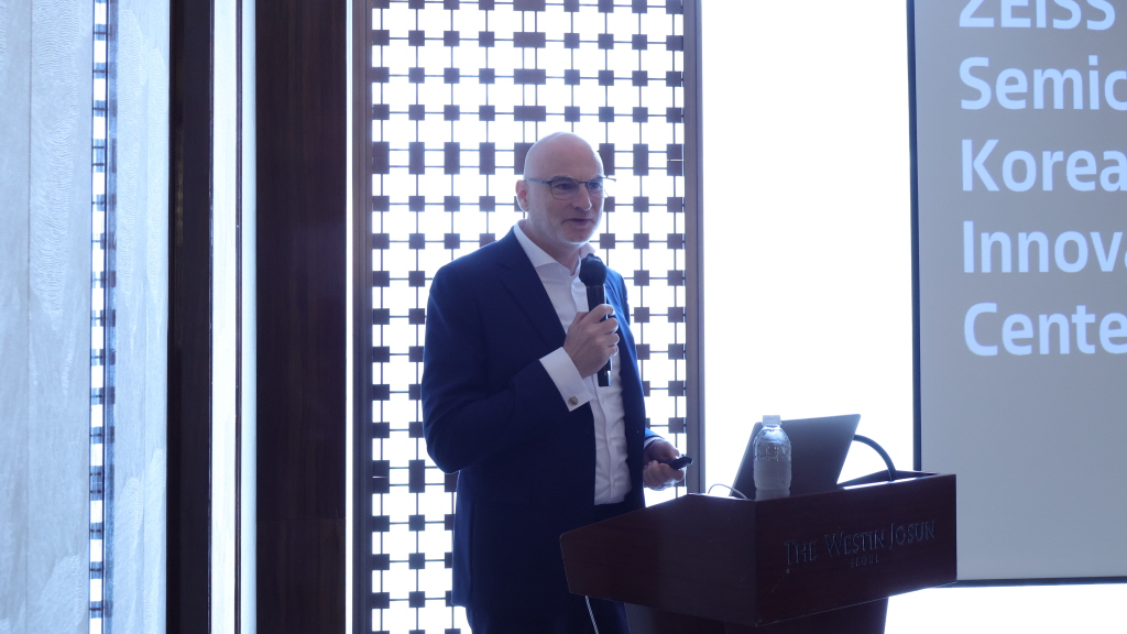
▲매튜 윌슨 자이스코리아 부사장이 발표하고 있다.
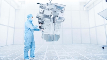
센터 규모는 총 350㎡로, 포토마스크와 웨이퍼 패키징 관련 자이스의 최신 솔루션을 갖췄다.
현재 센터에는 두 대의 장비가 설치돼 있으며, 세 번째 장비도 도입될 예정이다.
자이스 측은 센터가 동시에 네 대의 장비를 운용할 수 있도록 설계됐다고 설명했다.
다만 장비를 장기간 고정 배치하는 방식이 아니라, 고객사와 공동 개발을 진행한 뒤 일정 수준의 성숙도에 도달하면 고객 현장으로 이전하고 새로운 장비를 다시 들여오는 유연한 운영 모델을 구상하고 있다.
현재 센터를 기준으로 5개년 계획을 갖고 있으며, 향후 확장 가능성도 열어두고 있다.
자이스가 용인 센터에 우선 배치한 핵심 장비는 첨단 패키징 시장을 겨냥한 ZEISS NLX®-100과 ZEISS DUNE® 100이다.
NLX®-100은 인라인 3D 엑스레이 라미노그래피 기반의 계측·검사 솔루션으로, 복잡한 패키지 구조를 고해상도로 진단하고 데이터를 제공한다.
특히 마이크로범프, TSV 등 첨단 패키징 구조 내부의 결함을 비파괴 방식으로 확인할 수 있어 웨이퍼 레벨 및 첨단 패키징 공정에서 활용될 수 있다.
자이스는 NLX-100®을 통해 공정 개발팀과 엔지니어가 결함 정보를 바탕으로 공정 파라미터를 조정하고 장기적으로 수율 개선에 기여할 수 있다고 설명했다.
DUNE® 100은 웨이퍼 형상을 측정하고 교정하는 솔루션이다.
첨단 패키징과 3D 집적 공정에서는 금속층 형성, 본딩, 리소그래피 과정에서 웨이퍼가 휘거나 왜곡되는 문제가 발생한다.
이 같은 워페이지는 초점 오차와 평면 왜곡을 유발해 수율 손실로 이어질 수 있다.
DUNE® 100은 웨이퍼 전체뿐 아니라 특정 영역의 왜곡도 교정할 수 있으며, 화학 기계적 연마(CMP) 슬러리와 같은 화학 물질 없이 공정이 가능하다는 점을 강점으로 내세운다.
미하엘 헬첼 박사는 “DUNE®은 프리 본딩과 리소그래피 단계에서 웨이퍼 형상을 바로잡아 수율 향상을 지원할 수 있다”고 설명했다.
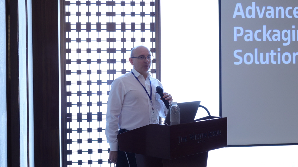
▲마하엘 헨첼 박사가 발표하고 있다.
자이스는 차세대 포토마스크 수리 장비인 ZEISS MeRiT AE도 한국에 도입할 계획이다.
MeRiT AE는 기존 MeRiT LE의 차세대 솔루션으로, 최첨단 공정에서 핵심 역할을 하는 포토마스크의 미세 결함 수리 능력을 확장한 장비다.
자이스는 이 장비의 첫 프로토타입을 한국에 들여와 고객사와 미래 공정 대응을 위한 협력을 진행하겠다고 밝혔다.
자이스가 한국에 이 같은 시설을 마련한 배경에는 AI 확산에 따른 반도체 산업의 구조 변화가 있다.
윌슨 부사장은 현재 반도체 시장이 “AI 슈퍼사이클”에 진입하면서 개발 주기가 빠르게 단축되고 있다고 진단했다.
특히 첨단 패키징은 미세공정 축소만으로는 해결하기 어려운 성능 향상 요구를 뒷받침하는 핵심 기술로 떠오르고 있다.
카롤리네 피그돈 박사는 자이스 반도체 제조기술 부문에서 반도체 제조 광학, 마스크 계측 및 공정 장비, 웨이퍼 팹 솔루션 등을 제공하고 있으며, 특히 웨이퍼 팹 솔루션은 검사, 계측, 결함 분석, 웨이퍼 형상 제어, 첨단 패키징을 지원한다고 설명했다.
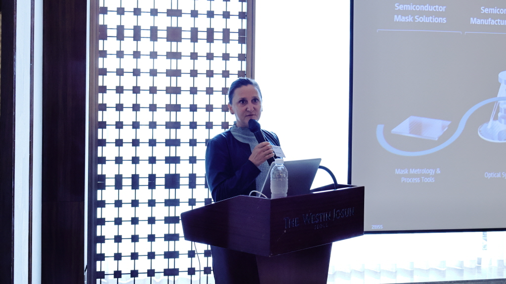
▲카롤리네 피그돈 박사가 발표하고 있다.
미하엘 헬첼 박사도 “첨단 패키징은 현재 업계에서 가장 뜨거운 주제”라며 “한국은 AI와 이종 집적 반도체 분야에서 중요한 생태계를 갖춘 시장”이라고 강조했다.
그는 NLX®-100이 향후 하이브리드 구리 본딩 등 차세대 패키징 로드맵에도 대응해야 한다고 설명했다.
다만 하이브리드 구리 본딩으로 갈수록 구조가 더 작아지고 엑스레이 해상도와 방사선 선량 관리가 중요한 과제가 된다고 덧붙였다.
자이스는 해상도 향상과 방사선 선량 저감을 핵심 로드맵으로 삼고 있으며, HBM 등 고부가 패키징 제품 보호를 위한 기술 개발도 병행하고 있다.
자이스는 센터를 단순한 장비 전시장으로 운영하지 않겠다는 방침이다.
고객이 직접 장비를 보고 시험할 수 있을 뿐 아니라, 자이스 본사 연구개발 인력과 한국 현지 인력이 함께 고객 공정에 맞춘 솔루션을 개발하는 협력 공간으로 삼겠다는 것이다.
윌슨 부사장은 “한국 고객사와 매년 여러 차례 로드맵 미팅을 진행하며 기술 영역 전반을 논의하고 있다”며 “센터는 고객과 함께 장비를 성숙 단계까지 발전시킨 뒤 실제 고객 현장으로 이전하는 방식으로 운영될 것”이라고 말했다.
한편 자이스는 약 180년 역사를 가진 독일 광학기업으로, 반도체 분야에서는 DUV·EUV 리소그래피 핵심 광학 모듈과 포토마스크 솔루션, 공정 제어, 소재 및 패키징 3D 분석·측정 포트폴리오를 보유하고 있다.

Comments
Related news
ZEISS Launches Three High-Resolution Image Processing Solutions for 3D Semiconductor Packaging Defect Analysis
Zeiss has announced three high-resolution 3D X-ray imaging solutions for failure analysis of advanced semiconductor packages, including 2.5/3D and fan-out wafer-level packages. The three new products, which are used for sub-micron and nano package FA operations, are the Xradia 600 Series Versa, Xradia 800 Ultra X-ray microscope, and the new Xradia Contexture MicroCT. By adding these products to its existing product line, Zeiss now offers an extensive portfolio of 3D X-ray imaging technologies for the semiconductor industry.
2019.01.23by 이수민 기자
ZEISS, “Korea is a key market”… Visit to Innovation Center
[Editor's Note] Zeiss Korea opened an Innovation Center last August, equipped with an advanced industrial equipment portfolio including optics, electronics, X-ray, microscopy, and 3D measurement systems. Zeiss Korea is contributing to the development of Korea's domestic industry through the supply of essential equipment for advanced sectors such as semiconductors, automobiles, and batteries. Accordingly, we participated in a tour of the Zeiss Innovation Center to explore Zeiss Korea's technological capabilities and future business strategies.
2022.11.30by 명세환 기자
[SEMICON Korea 2023] ZEISS to Unveil Latest EUV Photomasks and 3D Analysis Solutions at SEMICON
The global semiconductor industry exhibition 'Semicon Korea 2023' is just around the corner. At this annual venue where the growth of the semiconductor industry and the latest semiconductor manufacturing technologies can be confirmed, ZEISS Korea, a materials company that serves as a key component in EUV equipment, is also set to participate and showcase advanced technological capabilities.
2023.02.01by 명세환 기자
Zeiss Leads the Way in Sharing with the Underprivileged and Nurturing Future Generations
ZEISS Korea, a leading global optical company headquartered in Germany, is implementing various social contribution activities for underprivileged communities and future generations as the year draws to a close, practicing social value creation.
2023.12.07by 배종인 기자
Zeiss Korea to Participate in SEMICON Korea 2024
German company ZEISS Korea (CEO Jung Hyun-seok), a leader in the semiconductor materials sector, will participate in 'Semicon Korea 2024' to be held at Seoul COEX from January 31st to February 2nd.
2024.01.18by 배종인 기자











