



Next-generation semiconductor technology at a glance, from package substrates to neuromorphic devices… 2026 Semiconductor Business Performance Exchange Meeting
 Published2026.07.13 19:52
.jpg)
▲2026년도 반도체 사업 성과교류회 전경
공개 연구 AI 반도체 핵심 밸류체인 구성, AI 반도체 경쟁력 확보 기반 마련
인공지능(AI) 확산과 첨단 반도체 경쟁 심화로 차세대 반도체 기술 확보가 국가 경쟁력의 핵심 과제로 떠오른 가운데, 정부가 반도체 분야 연구 성과를 공유하고 산학연 협력 확대를 위한 교류의 장을 마련했다. 연구개발 성과를 산업 현장 수요와 연계해 실질적인 기술 경쟁력으로 이어가겠다는 취지다.
과학기술정보통신부는 13일부터 14일까지 부산 파라다이스호텔에서 ‘2026년도 반도체 사업 성과교류회’를 개최했다.
이번 행사는 과기정통부가 주최하고, 차세대지능형반도체사업단, 한국연구재단 외 12기관 주관으로 과기정통부가 지원하는 반도체 연구개발, 인력양성, 국제협력 분야 성과를 공유하는 행사로 올해 세 번째를 맞았다.
이번 행사에는 125개 연구과제 연구책임자를 비롯해 반도체 관련 기업과 기관 관계자 등 약 800명이 참석했다.
개회사에서 이강우 과기정통부 원천기술과장은 “전 세계적으로 반도체 기술 주도권 경쟁이 심화되는 가운데 연구과제 하나하나가 우리나라 미래를 좌우할 핵심 자산”이라며 “공유된 연구 성과가 세계 시장을 선도하는 새로운 기술로 이어질 수 있도록 연구자와 산업계가 함께 역량을 결집해 달라”고 말했다.
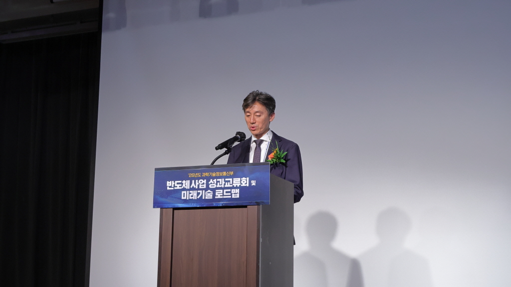
▲이강우 과기정통부 원천기술과장이 개회사를 하고 있다.

이어진 환영사에서 김형준 차세대지능형반도체사업단 단장은 “지난해 성과보고회 이후 1년간 소재·소자·공정·설계 등 다양한 분야에서 기술 발전과 산학연관 협력이 이뤄졌다”고 평가했다.
또한 “개별 과제의 성공만으로는 글로벌 기술 경쟁에서 우위를 확보하기 어렵다며, 연구 성과가 소재에서 소자, 시스템으로 유기적으로 연결되어야 혁신적인 K-반도체가 완성될 수 있다”며 “현장의 성과와 의견이 국가 반도체 R&D 정책 수립에 반영될 수 있도록 노력하겠다”고 밝혔다.
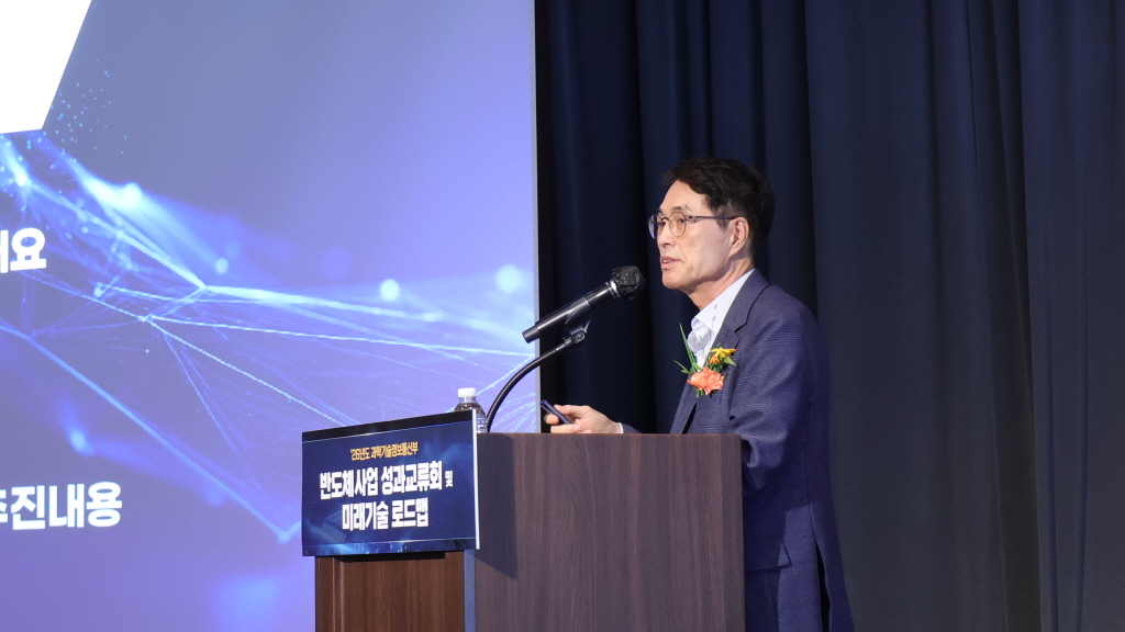
▲김형준 차세대지능형반도체사업단 단장이 환영사를 하고 있다.
행사 첫날에는 정소영 엔비디아코리아 대표가 기조연설자로 나서 ‘AI 팩토리(AI Factory)’와 관련한 산업 변화와 반도체 기술의 발전 방향을 발표했다.
정소영 대표는 AI를 단순한 기술이 아니라 에너지, 반도체, 인프라, AI 모델, 애플리케이션이 결합된 새로운 산업으로 설명했다.
특히 데이터센터가 단순 비용 센터를 넘어 ‘AI 팩토리’로 진화하며 새로운 가치를 창출하는 핵심 인프라가 되고 있다고 강조했다.
또한 대규모 AI 모델과 추론·에이전트 AI 확산으로 컴퓨팅 수요가 폭증하고 있으며, GPU뿐 아니라 CPU·메모리·네트워크 기술의 중요성도 커지고 있다고 밝혔다.
나아가 로봇, 자율주행, 스마트팩토리 등을 포함한 ‘피지컬 AI’가 차세대 성장 분야가 될 것이며, 제조업·반도체·IT 경쟁력을 갖춘 한국이 글로벌 AI 생태계에서 중요한 역할을 수행할 수 있다고 전망했다.
또한 전문분과 세션에서는 반도체 설계·인프라, 첨단 패키징, 나노소재, 화합물반도체 등 분야별 연구 성과와 향후 추진 방향이 공유됐다.
특히 고대역폭메모리(HBM) 확산과 첨단 패키징 수요 증가에 대응하기 위해 신소자와 첨단 패키징 분야 전문가 컨설팅도 진행됐다.
부대행사로 운영되는 반도체 성과 전시회에서는 최우영 서울대 교수의 ‘CMOS-NEM 임베디드 보안 엣지 인공지능 시스템’과 김민주 단국대 교수의 ‘메모리 인 센서 컴퓨팅 구현 및 검증을 위한 상온 3D 이종접합 기술’ 등 13개 주요 연구 성과가 전시됐다.
이 중 일부를 살펴보면 가장 먼저 주목되는 분야는 첨단 패키징이다.
심텍이 주관하는 ‘차세대 2.1D 반도체 패키지용 미세기판 개발’ 과제는 반도체 성능 향상의 중심이 칩 내부 미세화에서 패키징 기술로 이동하는 흐름에 대응한다.
과제는 선폭과 간격(Line/Space) 2㎛/2㎛ 수준의 수직 적층형 미세기판 구현을 목표로 한다.
포스터에 따르면 기존 기판의 회로 폭이 8∼12㎛ 수준인 데 비해 2.1D 기술은 1㎛ 이하 수준까지 미세화를 지향하며, 비아 크기 역시 36㎛에서 2㎛ 이하로 줄이는 것이 목표다.
이를 위해 미세회로 형성, 감광소재, 구리(Cu) 평탄화, 마이크로 비아 공정 등 핵심 기술을 병행 개발하고 있다.
이종집적 분야에서는 단국대학교 김민주 교수의 상온 3D 하이브리드 본딩 기술이 눈길을 끈다.
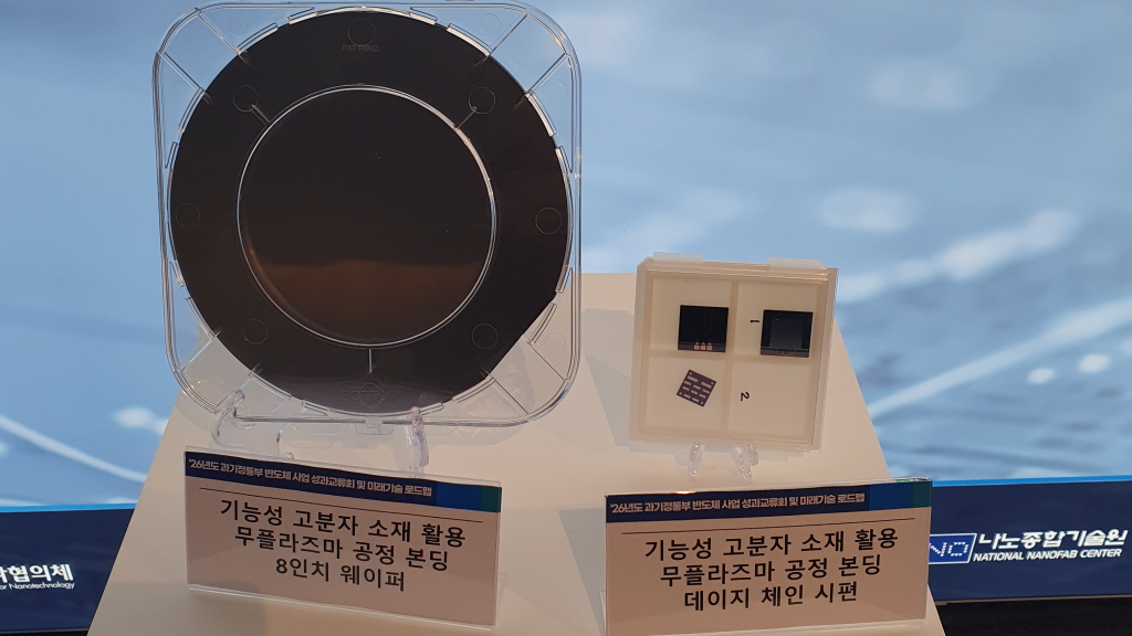
▲김민주 단국대 교수의 ‘메모리 인 센서 컴퓨팅 구현 및 검증을 위한 상온 3D 이종접합 기술’
연구진은 iCVD 공정으로 제작한 폴리머 기반 확산방지막을 활용해 40∼80℃ 수준의 저온에서 칩을 접합하는 기술을 개발하고 있다.
기존 방식과 달리 플라즈마 처리가 필요 없고 구리 확산 문제를 줄일 수 있다는 점이 특징이다.
연구팀은 이를 메모리-인-센서(Memory-in-Sensor) 구조 구현에 적용해 이미지센서와 메모리를 직접 결합하고, 온디바이스 노이즈 제거 기능까지 실증했다.
소자 분야에서는 이화여자대학교와 성균관대학교가 공동으로 개발 중인 3차원 시냅스 메모리 기술이 소개됐다.
연구진은 과거 NAND 플래시 메모리에서 문제로 지적됐던 트랩 전하에 의한 문턱전압 변화 현상을 오히려 활용해 인공지능 시냅스 기능을 구현했다.
제거 대상이었던 결함 특성을 학습용 메모리의 핵심 기능으로 전환한 셈이다.
연구진은 32단계 이상의 가중치 표현과 100만 회 이상의 프로그램·소거 내구성, 20년 이상의 데이터 보존 특성을 목표로 개발을 진행하고 있다.
서울대학교 최우영 교수가 주관하는 시스템 분야 연구는 연산과 보안을 동시에 해결하는 데 초점을 맞춘다.
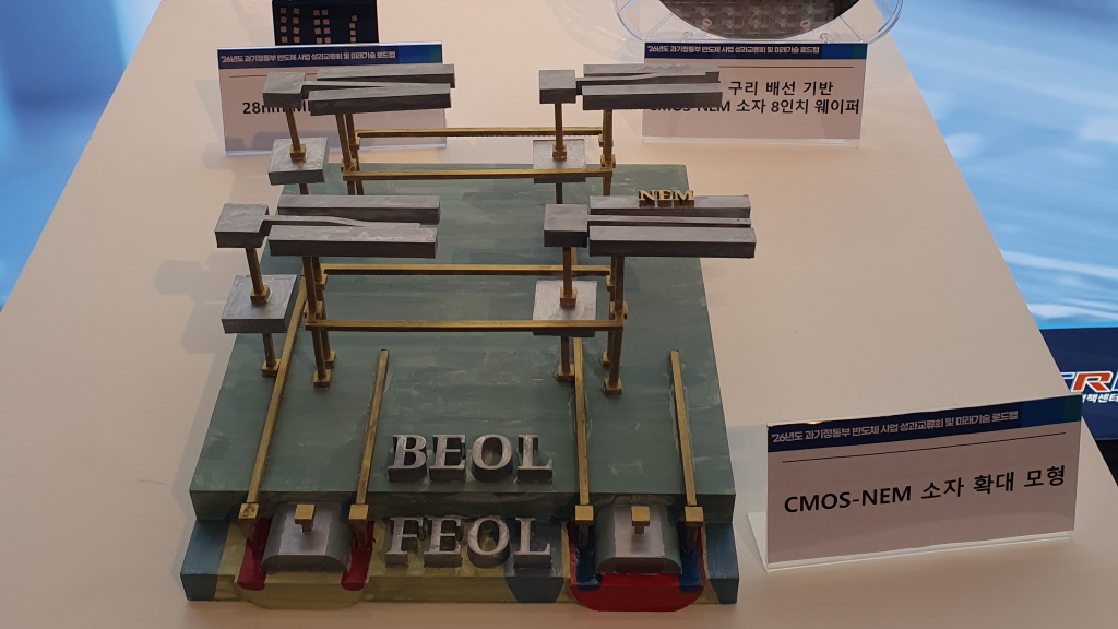
▲최우영 서울대 교수의 ‘CMOS-NEM 임베디드 보안 엣지 인공지능 시스템’
이 과제는 기존 컴퓨트인메모리(CIM)의 전력 소모 문제를 시간영역(Time-domain) CIM 구조로 개선하는 한편, 나노전자기계(NEM) 소자를 기반으로 한 물리적 복제방지함수(PUF)를 결합해 보안 기능까지 구현한다.
연구진은 임베디드 보안을 갖춘 1000 TOPS/W급 CIM 가속기 개발을 목표로 하고 있으며, NEM-PUF 구조를 통해 면적과 읽기 에너지를 크게 줄였다고 밝혔다.
이번 전시에서 독특한 위치를 차지한 것은 나노종합기술원의 MPW(Multi-Project Wafer) 기반 스케일업 플랫폼이다.
이 사업은 대학과 연구소 수준에서 개발된 AI 반도체 기술을 실제 제조 공정으로 연결하는 공용 인프라 구축이 목적이다.
CMOS 기반 회로와 차세대 메모리 소자를 단계적으로 통합할 수 있는 특화 MPW 플랫폼을 제공해 연구 성과의 사업화 가능성을 검증하는 역할을 맡는다.
이번에 공개된 연구들은 각각 다른 분야를 다루고 있지만, 전체적으로는 AI 반도체의 핵심 밸류체인을 구성한다.
소자 개발, 시스템 구현, 3차원 집적, 첨단 패키징, 제조 검증 인프라가 하나의 흐름으로 연결되면서 국내 AI 반도체 경쟁력 확보를 위한 기술적 기반을 구축하고 있다는 평가가 나온다.

Comments
Related news
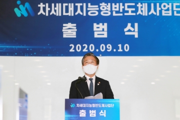
Launch of a Single Business Group Overseeing Next-Generation Intelligent Semiconductor Business
The Ministry of Science and ICT and the Ministry of Commerce, Industry and Energy held a launch ceremony for the Next-Generation Intelligent Semiconductor Business Division at the Semiconductor Industry Association located in Seongnam, Gyeonggi Province, and signed an MOU to develop next-generation intelligent semiconductors and build an ecosystem to support it. A total of 1.096 trillion won will be invested over 10 years in the next-generation intelligent semiconductor technology development project overseen by the business division.
2020.09.11by 이수민 기자
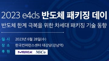
Overcoming semiconductor limitations is now packaging
Intel, Nexpak, Applied Materials, Hyundai Securities, Next-Generation Intelligent Semiconductor Business Division, and Hanyang University will host the "2023 e4ds Semiconductor Packaging Day," a specialized seminar on semiconductor packaging, on Wednesday, June 28 at the Grand Auditorium of Korea Conference Center.
2023.06.07by 명세환 기자
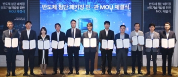
Semiconductor Advanced Packaging, Public-Private Partnership
The Ministry of Trade, Industry and Energy, Samsung Electronics, SK Hynix, LG Chem, Hana Micron, Protec, Sapion Korea, Simtec, the Next-Generation Intelligent Semiconductor Business Division, the Korea Semiconductor Industry Association, the Korea Institute of Industrial Technology Evaluation and Planning, and other companies in the materials, parts and equipment (MPM) sector, semiconductor advanced packaging specialists (OSAT), and fabless enterprises concluded an agreement on cooperation for semiconductor advanced packaging technology development.
2023.08.29by 배종인 기자
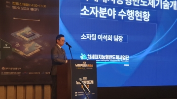
“Next-generation intelligent semiconductor, targeting 1 teraflops of computing efficiency by 2029”
Lee Seok-hee, team leader of the Device Team at the Next-Generation Intelligent Semiconductor Business Division, presented "2025 Next-Generation Intelligent Semiconductor Technology Development Project Device Sector Implementation Status" at the '2025 Neuromorphic Semiconductor Workshop' held at L Tower on the 19th. He stated, "Researchers aim to complete next-generation semiconductor technology with 1 teraflops of computational performance by implementing a prototype by 2029," and added, "To achieve this, foundational technology acquisition, core design, and platform construction will be carried out."
2025.05.26by 배종인 기자
.jpg)
Next-Generation Intelligent Semiconductor Technology Development Project Achieves 1,426 Patents and Creates 1,628 Jobs Over 5 Years
The Ministry of Science and Technology (Minister Bae Gyeong-hun) and the Ministry of Trade, Industry and Energy (Minister Kim Jeong-gwan) jointly hosted the "2025 Next-Generation Intelligent Semiconductor Technology Development Project Integrated Technology Exchange Conference" in Jeju for two days from October 27 to 28. The event was organized by the Next-Generation Intelligent Semiconductor Business Division (Director Kim Hyeong-jun), bringing together approximately 550 researchers from industry, academia, and research institutions representing Korea's semiconductor sector to share research achievements and technology trends while strengthening collaborative networks.
2025.10.27by 명세환 기자











