



The first signal determines the fate of the system
 Published2026.10.09 09:12
Technical Whitepaper
Measurement guide for root cause identification of boot failures: from power-on sequence analysis to clock quality measurement
Summary
This whitepaper, based on the presentation materials and technical Q&A from the WaveInsense webinar 'Power & Boot Sequence Measurement Know-how,' summarizes measurement techniques for the initial operation interval spanning from the power-on sequence (Power-on Sequence) to the boot sequence (Boot Sequence), clock stability, and DC power quality in embedded systems. It presents a measurement procedure for narrowing down the causes of intermittent boot failures from the perspective of power rail sequence, PGOOD, reset, and clock quality, and addresses measurement pitfalls such as aliasing, low-frequency attenuation in AC coupling, and probe ground loops along with avoidance methods. Finally, it clarifies the boundary leading to integrated verification of power integrity (PI) and signal integrity (SI).
1. Problem Definition: The Cause of Boot Failures Lies in the First Signal
Repeated system resets and intermittent boot failures occurring during product verification are often attributed to high-speed interfaces or software issues. However, upon actual analysis of root causes, problems frequently originate from the most fundamental initial operating conditions of the system—power integrity, power sequencing, reset, and clock signals. As a result, when debugging begins with high-speed signals or the software layer, the search extends to layers different from where the problem actually exists, and this cost escalates especially for intermittent failures that are difficult to reproduce.
Therefore, the starting point for debugging is to retrace the system initialization process step-by-step: stabilization of each power rail, reset release, clock preparation, and CPU startup. The question this document seeks to answer is simple: not whether voltage exists, but rather how to verify through measurement that power, PGOOD, reset, and clock are connected in the correct sequence and with adequate quality.
2. Power Path and Measurement Points in Embedded Systems
To narrow down the cause, one must first identify where power and signals meet. An embedded system consists of three sections: a power management block, a core processing and memory block, and a peripherals and driver block. In the power management block, AC input is converted through an SMPS (Switch Mode Power Supply) to a 12 V or 5 V DC bus, and a PMIC and LDOs generate functional rail voltages such as VDD_CPU (1.0 V), VDD_IO (1.8 V), VDD_DDR (1.2/0.6 V), and VDD_3V3 (3.3 V). These rails must be activated sequentially in accordance with predetermined timing and control signal schemes, with power sequencing logic managing Power On Sequence, Power Good Monitor, and Fault Protection (OVP/UVP/OCP/OTP).
Peripherals such as display backlighting, motor drivers, Ethernet, and camera modules consume relatively large amounts of power. Therefore, the design ensures that power is not applied to these until the system core completes booting and the OS stabilizes. This choice accepts the trade-off of delayed peripheral availability in exchange for blocking large transient currents from creating power disturbances during the boot interval.
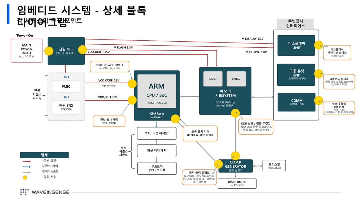
The principle for measurement points is as follows: first, verify compliance with specifications at the receiving point near the load IC. If anomalies are found, compare the same signal at the source and along the intermediate path to separate whether the problem originates from the source or from impedance, reflection, and PDN (Power Delivery Network) issues along the path. Figure 1 shows the measurement points across the entire power-on and boot sequence intervals. Core power ripple (less than 1% based on CPU pin), VDD_DDR ripple and DQ/DQS setup-hold timing margin, CLKOUT jitter, and PGOOD to RESET timing margin are critical measurement items.
3. Power-On Sequence and Boot Sequence: Sequence is Specification
Once measurement points are established, the next question is the standard for judgment. The power-on sequence (Power-on Sequence) is the hardware preparation process from the instant power is supplied to the system until the CPU reaches an executable state, while the boot sequence (Boot Sequence) is the software startup process from after CPU reset release until the operating system or application begins execution. If power and clock are not prepared stably, the boot sequence cannot start normally.
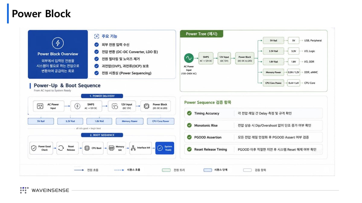
The power-on sequence proceeds through four stages: external power supply, power tree activation, power sequence timing, and clock/CPU stabilization. The boot sequence begins with reset vector fetch immediately after reset release and continues through boot device discovery, primary bootloader (SPL) loading, DDR initialization, full bootloader execution, driver initialization, and application startup. Only after the SPL initializes the DDR memory controller can the larger full bootloader and OS kernel be loaded. As a result, power and signal quality during the DDR initialization interval directly determines boot success.
The verification standard is not a single absolute voltage value. As shown in the verification items in Figure 2, judgment is based on four axes: timing accuracy of delays between each voltage rail (Timing Accuracy), monotonic rise without dips or overshoots during voltage rise (Monotonic Rise), PGOOD assertion after all rails stabilize, and appropriate delay-based reset release after PGOOD (Reset Release Timing). The reference values must be taken from the power sequence specifications in the datasheet of the device receiving the power. Therefore, rather than observing all rails simultaneously for long periods, a more efficient approach is to first synchronize the reference input, core power, PGOOD, and reset, then view them together across multiple channels.
4. Clock Stability: Phase Noise Consumes Timing Margin
Once the power rails have risen in the correct sequence, the next link is the clock. The clock is not merely a signal that generates frequency; it is the timing reference standard for all system judgments. CPUs and SoCs can achieve normal booting and control only after a stable clock is prepared, and PLL Lock signifies both convergence to target frequency and readiness for use of that clock domain. Therefore, during measurement, if a PLL status signal is available, it is beneficial to compare its relationship with reset and the actual clock output together.
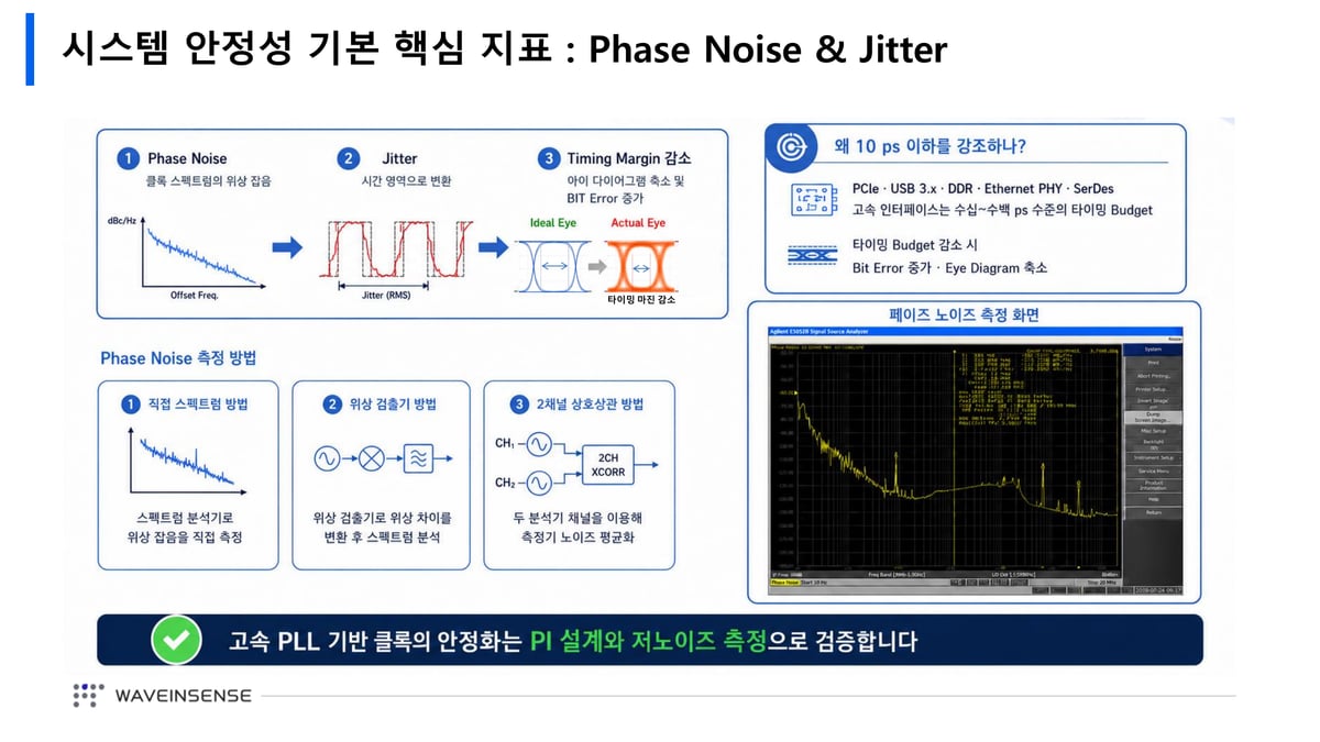
The key indicators of clock quality are phase noise and jitter. Phase noise in the frequency domain (dBc/Hz) manifests as jitter in the time domain (RMS), resulting in eye diagram shrinkage and increased bit errors. The timing budget for high-speed interfaces such as PCIe, USB 3.x, DDR, Ethernet PHY, and SerDes is on the order of tens to hundreds of picoseconds, so if jitter consumes this budget, operating margin disappears. The figures like 10 ps or less emphasized in the presentation should be understood as design criteria determined by the target system and data rate, rather than as universal standards.
There are three methods for phase noise measurement: the direct spectrum method, which directly observes phase noise with a spectrum analyzer; the phase detector method, which converts phase difference with a phase detector and then analyzes the spectrum; and the two-channel cross-correlation method, which averages the analyzer's inherent noise using two analysis channels. The cross-correlation method requires measurement channel configuration from two channels while reducing the impact of instrument noise. Figure 3 summarizes the causality from phase noise to jitter to timing margin reduction and these measurement methods.
5. Boot Interval Measurement: Separate Long Time Scale from High-Speed Clock
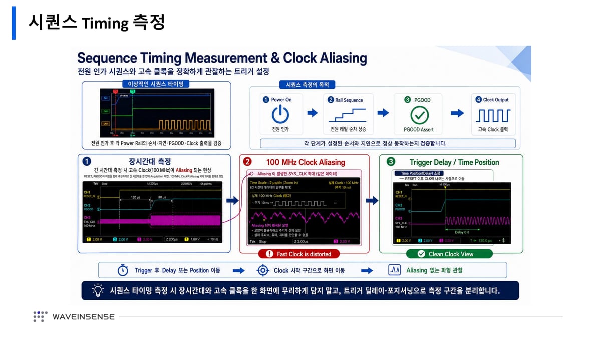
Even with established criteria and indicators, boot interval measurement has unique pitfalls. Verifying the power sequence order requires a long time axis, but if the same screen includes high-speed clock signals, the sample rate over that interval becomes insufficient, causing the clock to alias and display as a distorted waveform.
5.1 Aliasing and Measurement Interval Separation
In the slide examples, when measuring RESET and PGOOD timing over a long time scale while simultaneously acquiring a 100 MHz clock, the clock's appearance became irregular and its period appeared longer than actual, producing distortion. In this state, actual frequency, duty, and jitter cannot be judged. The solution is measurement interval separation. Adjust trigger delay or position to move the screen to the time point after reset where clock appears, and secure the necessary sample rate and memory depth for that interval. As a result, order verification and clock quality verification are split into two captures, increasing measurement instances, but enabling accurate judgment compared to distorted waveforms forced into a single screen. Figure 4 demonstrates this process.
5.2 TIE and Bus Quality Verification
TIE (Time Interval Error) is used to quantify clock quality. TIE is the cumulative time error of actual edges relative to an ideal reference clock, calculated as the difference between measured time at the Nth edge and N×T0 (ideal period). Positive values indicate the measured edge is delayed; negative values indicate it is advanced. Oscilloscopes with TIE analysis options automatically calculate error relative to the reference clock and histograms, while those without the option require manual readout using cursors and the ΔT menu. Manual measurement is possible without additional options but sacrifices automatic statistical analysis.
Verification of low-speed buses controlling the boot process follows the same principle. The essence of I2C measurement is verifying both signal quality of SCL/SDA and the sequence of Start-Address-ACK-Data-Stop together. Even if decoding results appear normal, failure to establish threshold level settings, sufficient sample rate and memory depth, and trigger setup based on Start condition, address matching, and data bytes can miss insufficient signal margin. Decoding is a tool for rapidly reading addresses and commands; waveform quality verification is separate work.
6. DC Power Quality: Judge Specification Compliance, Not Measured Values Alone
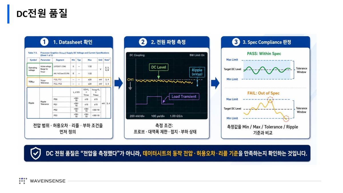
Even when sequence and clock are normal, the quality of the rails themselves can shake boot stability. DC power quality measurement does not end with the fact that voltage was measured. First define the datasheet's operating voltage, tolerance, ripple, and load conditions, acquire waveforms under conditions matching probe, bandwidth limiting, grounding, and load state, then judge by comparing measured values against Min/Max/Tolerance/Ripple criteria. Figure 5 demonstrates this three-step procedure.
6.1 Ripple: From Magnitude to Distribution and Frequency
Ripple is examined by first confirming actual DC level and total variation with DC coupling, then removing DC and observing with expanded detail under AC coupling. However, AC coupling, due to its high-pass characteristics, can attenuate and distort very low-frequency ripple and slow load changes. Gaining resolution of small ripple involves sacrificing some low-frequency information, so when judging slow changes, the DC-referenced waveform must be preserved. The judgment criterion is Vpp (Peak-to-Peak), with Max-Min viewed as reference.
Do not stop at ripple magnitude alone; also observe distribution and frequency. The dominant column in a histogram represents the typical ripple magnitude under normal conditions, while small columns at the periphery indicate anomalous distributions such as intermittent spikes or bursts. When anomalous distribution is observed, use FFT to confirm frequency components and analyze correlation with possible sources such as switching, clock, regulator operation, and EMI. The measurement location is primarily the point where voltage is actually used by the load, and comparing the regulator output, intermediate path, and load vicinity can more accurately narrow the generation interval.
6.2 Separation of Drop and Droop
Voltage Drop (IR Drop) is sustained voltage reduction due to DC resistance in PDN wiring and vias, expressed as the product of load current and path resistance. Conversely, Voltage Droop is instantaneous voltage reduction due to rapid current change rate and parasitic L and C, approximated as the sum of L×di/dt and I×R components. Since the causes differ, the responses differ as well. IR Drop requires checking path resistance and current—wiring, vias, and power distribution—while Droop requires examining load change rate, PDN impedance, decoupling placement, and regulator response. If problems are reproduced only during boot or memory initialization intervals, it is advantageous to suspect instantaneous Droop before average voltage.
Probe selection also branches according to measurement purpose. DC-DC output ripple calls for a frequency-domain approach observing switching frequency and harmonics, while CPU power (Vcore) ripple calls for a time-domain approach observing instantaneous dips and noise. Passive probes offer cost efficiency for general measurement, active probes provide wide bandwidth and low input capacitance, and power rail probes offer low-noise measurement and high common-mode rejection. Prioritizing versatility and cost points to passive probes; prioritizing resolution of fine ripple points to power rail probes. This is a trade-off relationship.
7. Measurement Environment Creates Fake Waveforms
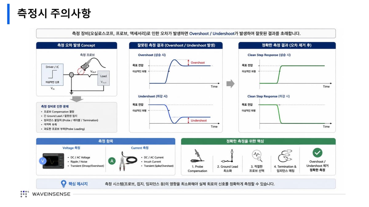
The premise for specification-based judgment is that measurement itself is correct. However, poor probe compensation, long ground leads and incorrect grounding, impedance mismatch between probe, cable, and termination, insufficient bandwidth, and excessive probe loading (Probe Loading) create overshoot and undershoot that do not exist in the actual circuit. Failure to check these measurement errors and directly applying results to debugging wastes time and resources chasing problems that do not exist.
A representative example is ground connection method. Using ground leads can make high-frequency spikes, ringing, and noise appear larger than actual, while using ground springs allows observing a cleaner waveform compared to leads. When actual waveforms are suspected of being circuit problems or measurement errors, measure using both leads and springs separately and compare. If necessary, cross-verify with different bandwidth settings or different probes. Figure 6 illustrates the structure of measurement error generation and the difference after removal.
High voltage power supply (HVPS) measurement requires dedicated probes as a prerequisite. High voltage probes provide safety attenuation, isolation design, and high input impedance, while optically isolated probes (Isolated Probe) provide high CMRR, ground loop elimination, and high dv/dt immunity. These should be viewed as measurement boundaries protecting the operator and grounded oscilloscope before waveform quality.
8. Boundary and Next Steps: Integrated Verification of PI and SI
Returning to the initial tension, boot problems are resolved not by the presence or absence of power but by observing whether power, PGOOD, reset, and clock are connected in correct sequence and quality. However, the scope of materials on which this document is based extends only to power quality and ripple/noise measurement under dynamic load conditions. High-speed interface and signal integrity (SI) measurement of system blocks falls outside the scope of this material and was announced as a topic for follow-up seminars. Differentiation of boot delays within the software domain—distinguishing between kernel space and user space—is also a boundary difficult to answer with measurement equipment, as clarified in Q&A.
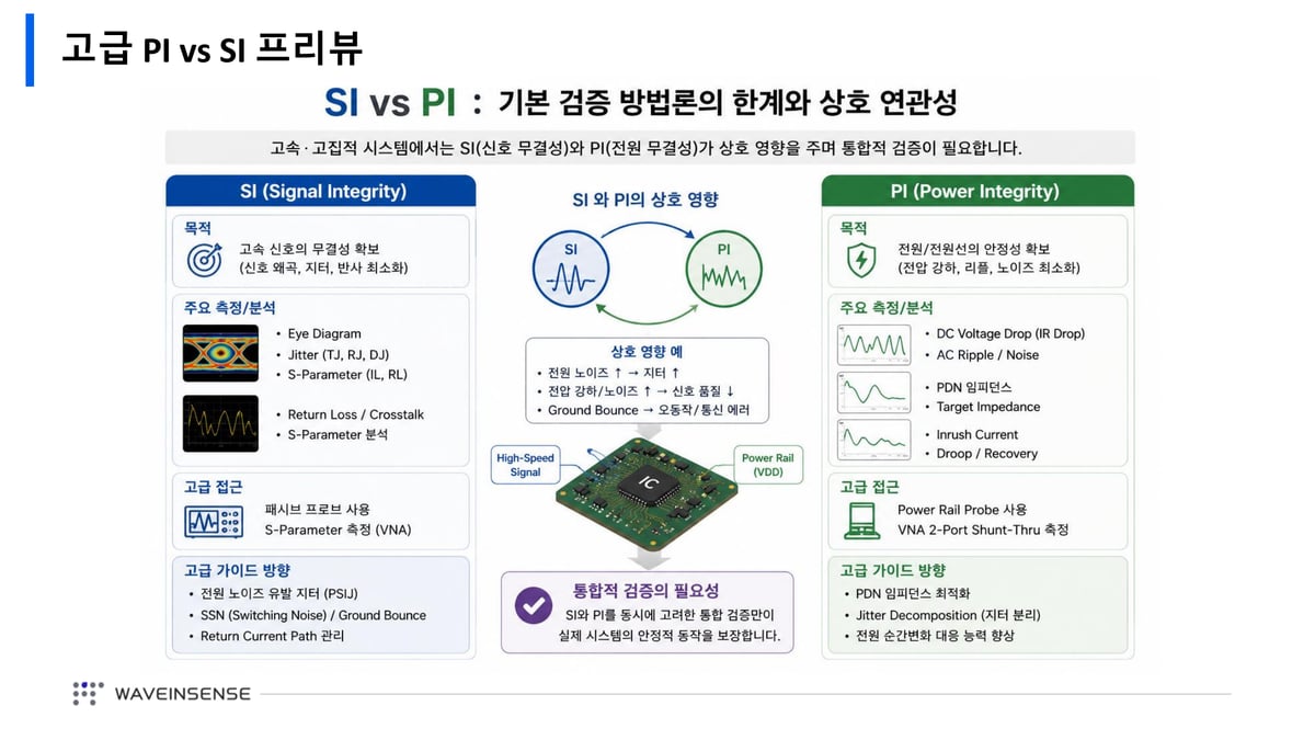
However, boundary does not mean disconnection. In high-speed, high-density systems, increased power noise leads to increased jitter, voltage drop and noise increase lead to signal quality degradation, and ground bounce leads to malfunction and communication errors. Therefore, integrated verification considering both SI (signal integrity) and PI (power integrity) simultaneously is necessary, and the phenomenon where individual verification passes at the equipment level but intermittent boot failures or data errors persist at runtime can be explained by this mutual interaction. Figure 7 summarizes this mutual relationship.
Advanced approach directions were presented as follows: on the PI side, use power rail probes and VNA 2-Port Shunt-Thru actual measurement to verify PDN impedance; on the SI side, deepen analysis through power supply induced jitter (PSIJ), simultaneous switching noise (SSN) and ground bounce, return current path management, and jitter decomposition. The measurement in this document confirming the sequence and quality of first signals becomes the starting point for integrated verification.
Appendix. Webinar Technical Q&A
- Q1. When debugging Power Sequence issues, not only must power rail rise time and sequence be considered, but also PGOOD, Reset, and Clock. Is there an actual effective measurement order for narrowing down the boot failure cause?
- Major power rails must be confirmed first. Since clock operation is difficult without power transmission, the subsequent effective measurement order is PGOOD signal, then clock quality.
- Q2. When measuring multiple voltage rails, where should the reference point for each rail be set?
- When there are multiple voltage rails, the GND of the rail being measured should be set as the reference point.
- Q3. What is the difference between ground lead method and ground spring method when measuring DC ripple and high-frequency noise?
- With ground leads, high-frequency spikes may appear larger or ringing and noise may appear larger. With ground springs, waveforms can be observed more cleanly compared to ground leads.
- Q4. Identical circuits, but boot time becomes longer or boot fails on certain boards during production. To confirm whether DC Ripple or Ground Noise is the cause, which Power Rail and interval should be measured as priority?
- Substantive response was not provided; individual consultation was recommended.
- Q5. When the ripple frequency of a power rail appears different from the switching frequency, how should the primary cause be traced?
- Substantive response was not provided; individual consultation was recommended.
- Q6. The CPU resets when a high-current motor operates, but no significant voltage variation is confirmed at the power supply. In this case, how should Ground Bounce or Ground Noise be measured in actual systems to distinguish between power and grounding issues?
- Substantive response was not provided; individual consultation was recommended.
- Q7. What reference standard should be used when verifying timing between multiple voltage rails?
- The datasheet of the device receiving the power rail must be confirmed. The reference should be set based on power sequence specifications in the documentation.
- Q8. When implementing power-on sequencing with Power Good signal and resistive divider instead of sequencer IC, how should timing margin reduction due to device aging and temperature change be verified by instrumentation?
- Substantive response was not provided; individual consultation was recommended.
- Q9. Power-on sequence falls within normal range, but significant ground bounce occurs at the moment system reset signal is released. Is this a power issue or crosstalk problem of digital logic signals, and what is the measurement procedure to distinguish?
- Substantive response was not provided; individual consultation was recommended.
- Q10. To experimentally confirm the path through which power rail noise transitions to clock jitter, what measurement configuration is most effective?
- Substantive response was not provided; individual consultation was recommended.
- Q11. During power integrity measurement, fine ripple at tens of mV level is often misidentified due to instrument noise floor of the oscilloscope. What is the method to clearly separate instrument noise from actual board DC ripple?
- Substantive response was not provided; individual consultation was recommended.
- Q12. When measuring IO bus quality, are templates or reference values/materials provided as benchmarks?
- The reference standard differs for each IO bus. If target bus and application information are provided, relevant materials will be provided individually.
- Q13. Are tools or simulators provided to preemptively verify mutual compatibility and improve measurement quality?
- For a response, detailed content on the target application must be confirmed. Upon submission of relevant content, a response will be provided after verification.
- Q14. Is vulnerability analysis also provided for DC power quality measurement?
- We aim to provide not just equipment distribution but solutions related to customer applications. Upon submission of content related to applications, analysis methods will be compiled and provided.
- Q15. When measuring clock jitter, how is instrument jitter separated from DUT-generated jitter?
- Substantive response was not provided; individual consultation was recommended.
- Q16. For interpretation of frequency anomalies, is guidance or recommendation provided on what types of anomalies seem likely?
- Anomalies can appear differently depending on the solution. If information on applications in progress is provided, relevant materials will be provided individually.
- Q17. When measuring PSIJ (Power Supply Induced Jitter) where clock signal jitter is coupled with power rail ripple, which instrument combination of oscilloscope and spectrum analyzer and what approach enable intuitive analysis?
- Substantive response was not provided; individual consultation was recommended.
- Q18. When measuring high-speed clocks, probe grounding or the measurement environment itself can create ringing or overshoot appearing as actual waveforms. What is the practical method to distinguish whether a measured waveform is an actual circuit problem or measurement error from the probe?
- Comparing measured waveforms using probe ground leads and ground springs respectively allows confirmation of whether measurement error exists.
- Q19. When analyzing a board that occasionally fails to boot after power application, what power rail should be checked first and what is the measurement order?
- CPU/SoC power rail should be checked first, followed by DDR and IO in sequence.
- Q20. A board intermittently fails to boot after power application, and voltage itself is measured within normal range. Can measuring EN to PGOOD delay or Reset Vector Fetch timing in Power Sequence distinguish causes, and what signal should be used as the reference for confirmation?
- Substantive response was not provided; individual consultation was recommended.
- Q21. Under what circumstances is the FFT/spectrum analysis function of an oscilloscope more suitable versus a spectrum analyzer?
- Substantive response was not provided; individual consultation was recommended.
- Q22. Are there new AI-related technologies for reducing instrument measurement error and automating measurements?
- To date, software enabling AI to connect and recognize instruments and verify feasibility of tests to be conducted does not appear to exist. However, programs for specific manufacturer solutions are provided.
- Q23. Even if power rail rise time satisfies datasheet conditions, what are the causes of actual boot failure in systems and what are measurement methods?
- Substantive response was not provided; individual consultation was recommended.
- Q24. In small-to-medium enterprise environments where significant PCB changes are difficult, when PI issues are confirmed, should power section component changes or PCB layout modifications be reviewed first? Explanations based on actual improvement cases are desired.
- Substantive response was not provided; individual consultation was recommended.
- Q25. When measuring Ground Noise, how are actual potential differences within the board distinguished from noise induced by probe ground loops?
- Substantive response was not provided; individual consultation was recommended.
- Q26. When validating sequencing of 8 or more power rails simultaneously using a multichannel oscilloscope, are there practical tips to prevent timing resolution loss due to horizontal axis scale settings?
- Substantive response was not provided; individual consultation was recommended.
- Q27. Power ripple normally shows no issues, but becomes larger only during boot. Can this phenomenon be the cause of boot failure?
- Substantive response was not provided; individual consultation was recommended.
- Q28. If boot failure is not reproduced and occurs intermittently, perhaps once in several dozen attempts, what trigger conditions should be set in the oscilloscope for effective results?
- First, using Pulse-related triggers is helpful.
- Q29. If Power-up Sequence timing specifications stated in SoC/FPGA datasheets are exceeded, is the chip unconditionally damaged, or does only boot fail?
- Substantive response was not provided; individual consultation was recommended.
- Q30. Power rail sequence is correct, but Power Rail Ramping Slew Rate is too fast or too slow. What problems occur and what are remedies?
- Substantive response was not provided; individual consultation was recommended.
- Q31. In multi-core processors, how is microsecond (µs) level timing difference between each Core Power and I/O Power precisely measured?
- Substantive response was not provided; individual consultation was recommended.
- Q32. When simultaneously measuring multiple channels (8 channels or more) of power lines and multi-digital signals, are there tips for oscilloscope trigger settings?
- Substantive response was not provided; individual consultation was recommended.
- Q33. What is the de-embedding method to minimize probe Ground Loop noise when measuring Power Rail?
- Substantive response was not provided; individual consultation was recommended.
- Q34. How is boot delay quickly determined to be caused by hardware initialization and kernel driver load (Kernel Space) versus background services and daemon execution (User Space)?
- The relevant content falls within the software domain, making it difficult to provide answers from an instrumentation perspective.
- Q35. What measurement settings are required to trap the instantaneous occurrence of Inrush Current and Voltage Sag simultaneously?
- Substantive response was not provided; individual consultation was recommended.
- Q36. What specialist technical expertise, capabilities, or work experience do personnel need to effectively apply and utilize practical measurement cases of Power & Boot Sequence? Interest is also expressed in specialized application strategies for automotive component suppliers and expected benefits.
- Theoretically, understanding of power architecture is necessary; practically, probing technique is required. Automotive component supplier specialized strategies have broad scope, so individual guidance based on relevant application information will be provided.
- Q37. When the same power rail shows different ripple and noise magnitudes depending on measurement location, which point should be used as the reference?
- The point where voltage is actually used by the load should be used as the reference. More accurate understanding can be achieved by comparing the regulator output, intermediate path point, and load vicinity points.
- Q38. When measuring ripple, is it sufficient to consider only Pk-Pk measured on the scope, or must Max-Min also be considered?
- Vpp should be viewed as the reference, with Max-Min considered as reference only.
- Q39. When confirming correlation between PI and SI issues, what waveform should be compared first?
- Substantive response was not provided; individual consultation was recommended.
- Q40. When measuring high-frequency noise generated immediately near MCU or AP power pins, is there a probing technique that completely eliminates disturbance noise induced by board ground loops?
- Substantive response was not provided; individual consultation was recommended.

Comments
Related news

Samsung Electronics, First Quarterly Operating Profit of 100 Trillion Won in Company History
Samsung Electronics surpassed 100 trillion won in quarterly operating profit for the first time in company history in its third quarter provisional results for 2026, demonstrating the expansion of AI investment.
2026.10.08by 배종인 기자

"Cooling is no longer just a mechanical issue"… ADI targets data centers with CDU control board
As AI server power density exceeds the limits of air cooling, data center cooling discussions have shifted from fans and heatsinks to liquid cooling and CDU configurations. With Nvidia's GB200 rack consuming 120kW and its successor GB300 in the 140kW range, approximately 100kW per rack represents the practical upper limit of air cooling. This year, LG Electronics and Autech Carrier entered complete product competition with Nvidia certification and marketplace listings, and demand is flowing down to sensor and control units below that tier. Noh Byun-ho, manager at Marktechnika Korea, says cooling has evolved from mechanical equipment into a measurement and control issue. While a pump handles pushing water, sensors and controllers determine how much to push. ADI constructed a CDU demo with tanks, pumps, valves, and cold plates actually connected together. Rather than a finished product, it is an evaluation platform that customers use as a development baseline. A single 10cm board handles control, converging sensor interfaces and driving pumps, fans, and valves while communicating with higher-level systems via Ethernet. PLCs are proven and advantageous at the prototype stage, but as production scales up, I/O and communication modules are added, and BOM, wiring, and equipment size all increase together. Power redundancy, hot-swap capability, and leak alarms are prerequisites, not features. However, determining the point at which to establish the infrastructure remains the responsibility of the designer's algorithm.
2026.10.06by 명세환 기자
AI-Driven Transformation of Power Semiconductor Landscape: Shift of Focus from Electric Vehicles to Data Centers
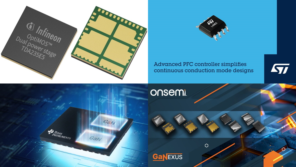
Power semiconductor demand is rapidly shifting from electric vehicle-centric applications to AI data centers and AI servers. With rising power consumption in AI servers, competition for high-efficiency GaN solutions has intensified, leading Infineon, ON Semiconductor, and TI to launch high-density and integrated products. Meanwhile, in the electric vehicle sector, SiC adoption is being strengthened through the expansion of 800V platforms. As a result, AI infrastructure expansion is becoming a key variable in future power semiconductor technology and investment.
2026.10.06by 배종인 기자
Microchip and Navitas Jointly Develop 800V DC Reference Design for AI Data Centers
Microchip Technology and Navitas Semiconductor have jointly developed a reference design for 800V DC power architecture for AI data centers. By combining GaN power devices, digital power controllers, and security ICs, it supports the OCP 800V DC standard and achieves maximum efficiency of 96% and power density of 2,100W/in³ through single-stage conversion.
2026.10.06by 배종인 기자
Gigaphoton Develops Neon Gas Recycling System for ArF Excimer Lasers...Achieves 50% Recycling Rate
Gigaphoton announced that it has developed a gas recycling system for ArF excimer lasers and achieved a 50% neon gas recycling rate.
2026.10.02by 배종인 기자











