


Please call it battery integrated management targeting IoT products, not just a simple battery IC.
 Published2015.10.12 21:07
TI Korea is launching bq25120, a highly integrated battery management solution for wearables and the Internet of Things (IoT).
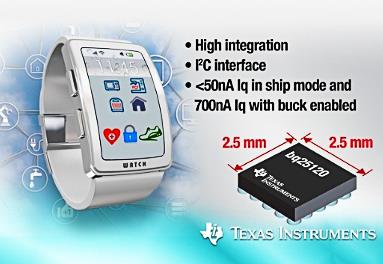
The bq25120 integrates linear charging, a configurable LDO, a load switch, a buck converter, pushbutton control, and battery voltage monitoring all into a single chip. Supporting batteries from 3.6V to 4.65V and fast charging currents from 5mA to 300mA, it enables "always-on" functionality in wearable and Internet of Things (IoT) applications without draining the battery. Additionally, it operates at 1.8V using a buck converter and optimizes battery life by reducing power consumption, with a quiescent current (Iq) of 700nA, the smallest in the industry.
 Byung-Nam Ahn, a manager in charge of the power sector at TI Korea, states that the new bq2512 chip is a battery integrated management solution targeting wearables and IoT products rather than a battery charging IC. We hear a detailed explanation of the bq25120 chip from Manager Ahn.
In terms of applications, the bq25120 is applicable to IoT as well as Bluetooth headphones, Bluetooth headsets, and health wearable devices with built-in heart rate sensors (HRM). Because wearables are smaller than conventional smartphones or tablets, they require smaller battery capacities. Therefore, a battery management solution suitable for this is necessary. In fact, current charging ICs from semiconductor manufacturers are primarily focused on smartphones, so their charging currents are typically 1A to 2A or higher. High performance cannot be expected from such charging ICs for IoT or wearables. This is because the total battery capacity of a wearable is typically only around 200mA to 300mA. Thus, a solution suitable for wearables is needed that achieves high efficiency and performance under such light loads.
The bq25120 adds many additional features to the basic functions of existing wearable charging ICs, such as the power path. One of these additional features is the integration of a 1.8V DC/DC converter block to supply system power, eliminating the need for users to design and incorporate a separate DC/DC converter. The output voltage can be adjusted from 1.1V to 3.3V, and the standby mode current is only 50nA. This is an important factor in ensuring a long battery life.
The DC/DC converter integrated into the bq25120 utilizes TI's proprietary control method known as 'direct control seamless.' This control method combines two techniques—voltage mode and hysteresis control—and offers the advantage of very fast load response characteristics. Furthermore, it guarantees approximately 80% of system performance even under light loads of 10uA or less. Since the switching frequency has been increased to 3MHz, users can configure smaller output LC filters. Thanks to this high-performance buck converter, the system has the advantage of being able to be minimized.
The default voltage is 1.8V, but this IC can adjust the output voltage in steps of approximately 100mV, for example, from 1.1V to 3.3V, by communicating with an AP or microprocessor through the I2C interface. By stepping up and down the output voltage in such 100mV increments, the AP can set and use a voltage more suitable for the system, allowing the user to configure the entire system more intelligently.
The quiescent current is also very small at 700nA. Reducing the quiescent current to below 1 uA is not an easy task, and the bq25120 offers a very low quiescent current even within the TI product family. Such a reduction in quiescent current increases overall system efficiency, extending the battery life of wearables and IoT products.
In addition, a pushbutton controller is integrated. This allows the AP to control the reset function as well as the manual reset function to turn the system on and off, thereby further extending battery life.
In addition, the bq25120 also integrates a voltage monitoring block that detects battery voltage.
From the perspective of the charger, which can be considered the main function, the charger voltage can be set via an external circuit or through I2C communication with the AP. Of course, the charging current can also be set externally or controlled via I2C. In terms of circuit protection, the input current limit can also be set externally or via I2C.
Another feature added to the bq25120 is an LDO that functions as a load switch. In the case of wearables, there may be systems that need to be powered on at all times, but for example, in BLE or wireless applications, systems that are powered on only when communicating are required. In such cases, a connection can be made via an LDO, and the output voltage can be provided only when needed.
Another point emphasized in the bq25120 is that the termination current has been lowered to 500uA. This represents a significant technological advancement that allows the full capacity of the battery to be utilized, even when using a very small battery. Another important point is the high accuracy of the termination current. Since the absolute level of the termination current is low and accurately managed, the battery can be used sufficiently and for a longer period.
In addition, the bq25120 also guarantees a shipping mode of 50nA. This means that the IC internally controls the path from the battery to the entire system.
The bq25120 is quite small, measuring 2.5mm x 2.5mm. It is difficult to find specialized solutions with a charging current of around 300mA in the current market. Even if such solutions exist, they tend to be larger than the bq25120. The fact that it integrates functions such as a power path, DC/DC converter, and LDO while remaining 2.5mm x 2.5mm in size is a significant advantage, especially for wearables where size is critical.
"As such, the bq25120 can be seen as having become a PMIC by integrating various functions within the IC. As the trend of accessories continues to grow, the number of designs using this wearable-specific IC as a discreet solution is expected to increase," said Manager Ahn.
관련뉴스
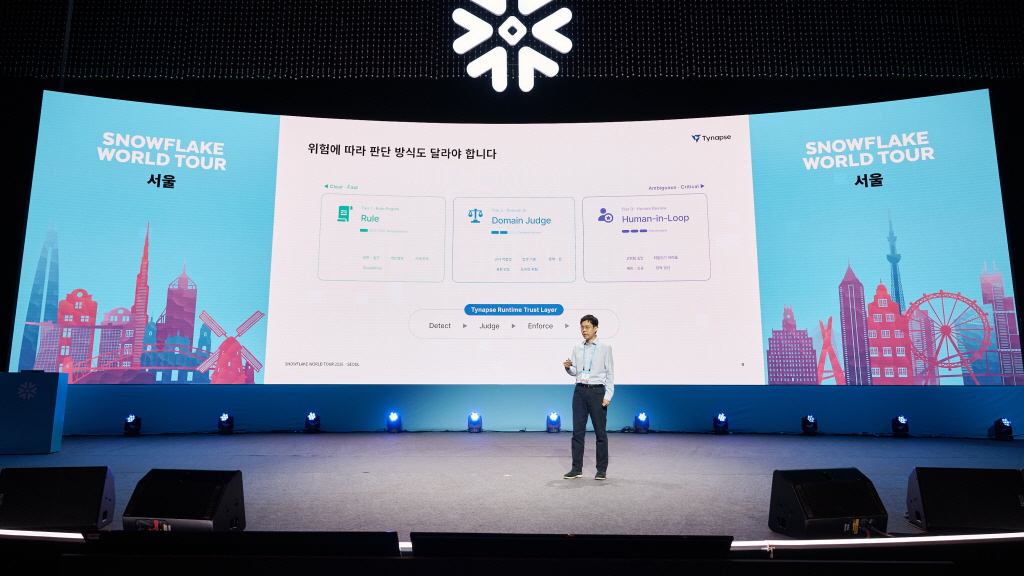
The Problem with AI is Not Performance, but Trust
CEO Kang Min-seung emphasized at Snowflake's World Tour Seoul that generative AI has entered a phase where "trust" rather than accuracy becomes the key competitive advantage. As AI is applied to various tasks including consultation, risk management, and operational automation, incorrect data, erroneous responses, and bias are creating actual business risks. He pointed out that enterprises must build a trust layer above AI. To achieve this, accurate data management, semantic structuring, governance, and prompt security are essential. He explained that AI is not merely an automation tool but a technology that reorganizes the entire organization's workflows and decision-making systems. Snowflake provides a platform that supports this trust-based AI operation, emphasizing that enterprises should build "trustworthy AI" rather than "intelligent AI."
2026.08.28by 배종인 기자
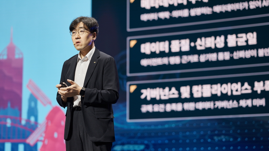
The Decisive Factor for AI Agents in Finance: "Trustworthy Data Infrastructure"
The key to spreading AI agents in the financial sector is establishing a trustworthy data system. KB Kookmin Bank is operating over 100 AI agents by 2025 and is promoting expansion to 300. AI is automating repetitive tasks across various areas such as consultation, risk management, wealth management, and relationship management. However, if data quality, governance, and semantic structuring are insufficient, errors and risks increase. KB is building an AI-Ready organization through a multi-model strategy of GPT, Gemini, and Claude, as well as a Snowflake-based data system. The bank emphasized that AI has entered a phase where it restructures not just simple automation but the entire work process and decision-making system.
2026.08.28by 배종인 기자
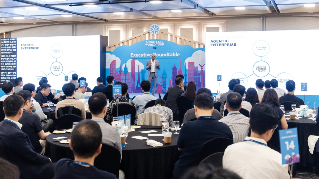
Snowflake Presents Data Platform Roadmap for Agentic AI Era
Snowflake emphasized at the Seoul roundtable that the key to enterprise AI proliferation lies in "Agentic AI" and the integration of data and workflows. Bala Kasivisvanathan stated that AI is evolving beyond simple analytics to become the driver of task automation and operational optimization, and that organizations must strengthen their data quality, processes, and governance as prerequisites for this. CJ OliveNetworks introduced that it is currently expanding AI applications in logistics and operational automation. Snowflake stressed that companies need a strategic shift to connect AI adoption to tangible business impact.
2026.08.28by 배종인 기자
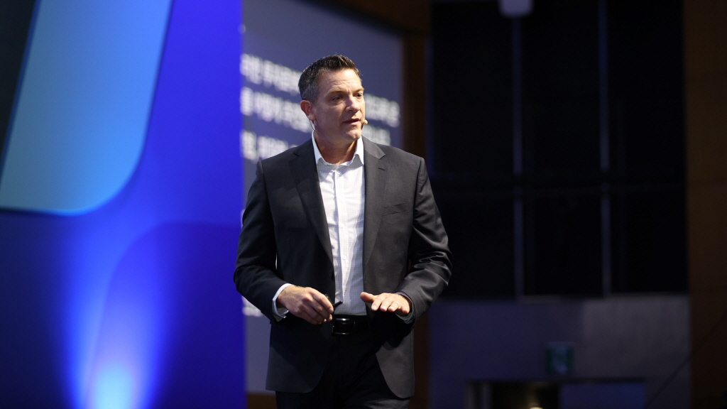
"All office workers will become agent managers"
At the Dell Technologies Forum 2026, Matt Dunfee, Senior Vice President at Dell Technologies headquarters, forecast that in the AI era, every worker will take on the role of managing dozens to thousands of agents, and emphasized that rather than simply adding AI to existing tasks, processes themselves must be redesigned. He pointed out that the success or failure of AI adoption depends not on technology itself, but on cost efficiency, data preparation, and AI economics, prototyping, and change management.
2026.08.28by 배종인 기자
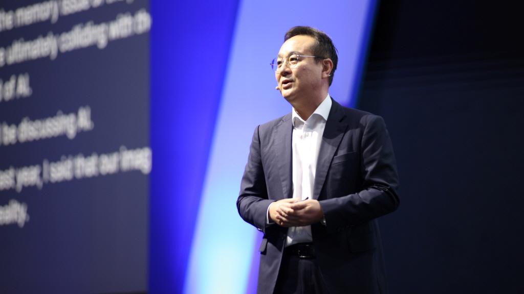
Sang-Mo Yu, Dell President: "AI Is Now Infrastructure—Integrated Approach to Security, Power, and Data Centers Is Essential"
At Dell Technologies Forum 2026, Sang-Mo Yu, President of Dell Technologies Korea, emphasized that AI has transcended the role of a productivity tool to become core infrastructure for enterprises and everyday life, underscoring the necessity of a hybrid AI infrastructure strategy integrating power, cooling, security, and data centers. He disclosed that he utilizes more than 20 AI agents daily and identified embedded security and the absence of unified roadmaps as major challenges for enterprises.
2026.08.28by 배종인 기자











