


Infineon Launches CoolMOS C7 650V Gold Combining Superjunction Process and Advanced SMD Package
 Published2016.06.03 06:20
Infineon Technologies AG (Korea CEO Seung-Soo Lee) has launched CoolMOS™ C7 Gold 650V in a TO-Leadless package.
This new product combines advanced superjunction (SJ) semiconductor processes with advanced SMD package design to deliver superior performance in hard switching applications. The package’s small footprint provides power density advantages for server, telecom, and solar applications.
C7 Gold CoolMOS technology with 4-pin Kelvin source capability and improved thermal characteristics in a TO-Leadless package enables rational SMD solutions for high current topologies such as power factor correction (PFC) up to 3 kW.
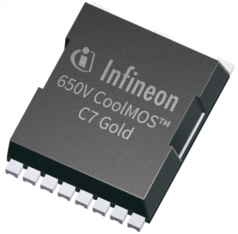
Additionally, the improved performance of C7 Gold delivers higher efficiency while reducing switching losses and heat dissipation. C7 Gold technology delivers the industry’s lowest unit area on-resistance Ron*A and a small size of just 115 mm², resulting in the lowest RDS(on) power density achievable in such a small footprint, at 33 mΩ.
The TO-Leadless package offers a 30% reduction in footprint compared to other conventional SMD packages such as the D²PAK, with a 50% and 60% reduction in height and space. The package can also be connected using a standard 3-pin MOSFET or a 4-pin Kelvin source approach. This provides the additional benefit of increasing efficiency, especially at full load, and makes the device easier to use by reducing ringing at the gates.
The high-quality TO-Leadless package has a very low source inductance of 1 nH, is lead-free and is MSL1 compliant. It also provides easy visual solder inspection and is suitable for wave and reflow soldering. Compared to through-hole packages, TO-Leadless has many advantages beyond high power density. The simple mounting process of the SMD package enables cost savings in manufacturing.

Comments
Related news
Infineon Announces Design Kit to Help with Easy and Fast Design
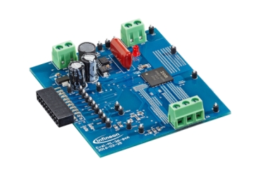
Infineon Technologies (Korea Representative Director Lee Seung-soo) announced the launch of the iMotion™ Modular Application Design Kit (MADK). This compact and highly flexible evaluation system provides a scalable design platform for three-phase motor drives with capacities ranging from 20W to 300W. The design kit consists of a controller board and a power board, and operates in sensorless mode, though sensors can optionally be used. Using this design kit allows engineers to implement a fully functional motor system within one hour, thereby shortening the product time-to-market. Designers can drive motors in just a few steps: connect the card to a PC, motor, and power supply, download and install the software, and adjust the parameters.
2016.05.12by 명세환 기자
Infineon Announces Power Modules Providing High Power Density for Hybrids and Electric Vehicles
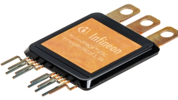
Infineon Technologies (Korea CEO Lee Seung-soo) has launched HybridPACK™ DSC (Double Sided Cooling), its latest power module product line for hybrid and electric vehicles. The new power module is offered in a very compact size of just 42mm x 42.4mm x 4.77mm. It targets HEV applications such as drive inverters and generators in the 40 to 50kW general power range, and can be used in parallel configuration to support higher power levels.
2016.05.18by 명세환 기자
Infineon Announces Innovative Silicon Carbide (SiC) MOSFET Technology
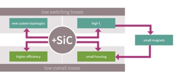
Infineon Technologies (Korea Representative Director Lee Seung-soo) has announced innovative silicon carbide (SiC) MOSFET technology that enables product designs to achieve previously unattainable levels of power density and performance. Infineon's CoolSiC™ MOSFET provides a new level of flexibility in increasing efficiency and frequency. This technology allows power conversion system developers to save space and reduce weight and cooling requirements while improving reliability and reducing system costs.
2016.05.23by 명세환 기자

Intel Unveils Next-Generation 'Core Ultra Series 3' and vPro Platform for Enterprise PCs
Intel has officially unveiled the "Intel Core Ultra Series 3" for next-generation enterprise PCs and the latest vPro platform, addressing a wide range of demands from enterprise notebooks to high-performance workstations.
2026.03.26by 배종인 기자

ROHM Launches ESD Protection Diode Compatible with High-Speed Interfaces of 10Gbps or Higher
Semiconductor specialist ROHM has developed the 'RESDxVx series' of ESD (electrostatic discharge) protection diodes capable of responding to next-generation high-speed data communication environments exceeding 10Gbps, simultaneously enhancing both signal quality maintenance required in high-speed interfaces and IC protection performance.
2026.03.26by 배종인 기자











