



Will domestic CPU cores bloom in the IoT era?
 Published2017.05.22 15:03
Director Song Yong-ho: "Confirmed potential for utilization in various fields"
The first phase of domestic CPU development, which began in June 2015, has entered its final stages. On the 19th, the "Second Domestic CPU Core Roadshow" was held to introduce the achievements of the "Domestic CPU Core Commercialization Project." Over one year, what new cores were developed and what results were achieved?
Ha Sang-tae, head of the System and Materials Industrial Technology Division at the Korea Institute of Industrial Technology Evaluation and Planning, said, "There are still negative views on domestic CPU development, but various institutions are producing results," adding "positive effects are expected in securing product competitiveness for 'Things' corresponding to IoT (Internet of Things), where hyper-connectivity and intelligence are being realized." Song Yong-ho, director of the Intelligent Semiconductor Promotion Division, said, "We confirmed the potential for domestic CPUs to be utilized in various ways," and "continuous attention must be paid to development."
The domestic CPU core roadshow introduced ADchips' ARK (revised name of emCore), ETRI's Aldebaran, and KETI's MENSA core, the same as last year. SoC development cases using cores included low-power mobile healthcare by Hancom GMD (ARK), tampering prevention and security-enhanced smart meters by S&A (Aldebaran), and voice recognition with built-in ultrasonic data communication capability by Emtec Vision (MENSA), discussing the advantages and disadvantages experienced using domestic CPUs.
ADchips announces ultra-lightweight CPU core
"We are introducing an ultra-lightweight 32-bit CPU core optimized for IoT developed through three years of research," said Lee Hee, vice president of ADchips, introducing the JUNO S0 and S1 processors, upgraded versions of the company's SE3208. "It is similar to how ARM upgraded the Cortex M0 to M0+, raising the pipeline to 2-stage to increase energy efficiency," he emphasized the ultra-lightweight and low-power characteristics suitable for application fields requiring 8-bit and 16-bit processors. Compared to existing models, encryption instructions are equipped, and the differences between JUNO S0 and S1 are that GPR counts are 8 and 16 respectively, MPU is absent and present, CPU cache is absent and present, and gate counts differ at 10,000 and 14,000.
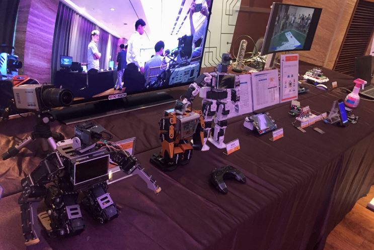
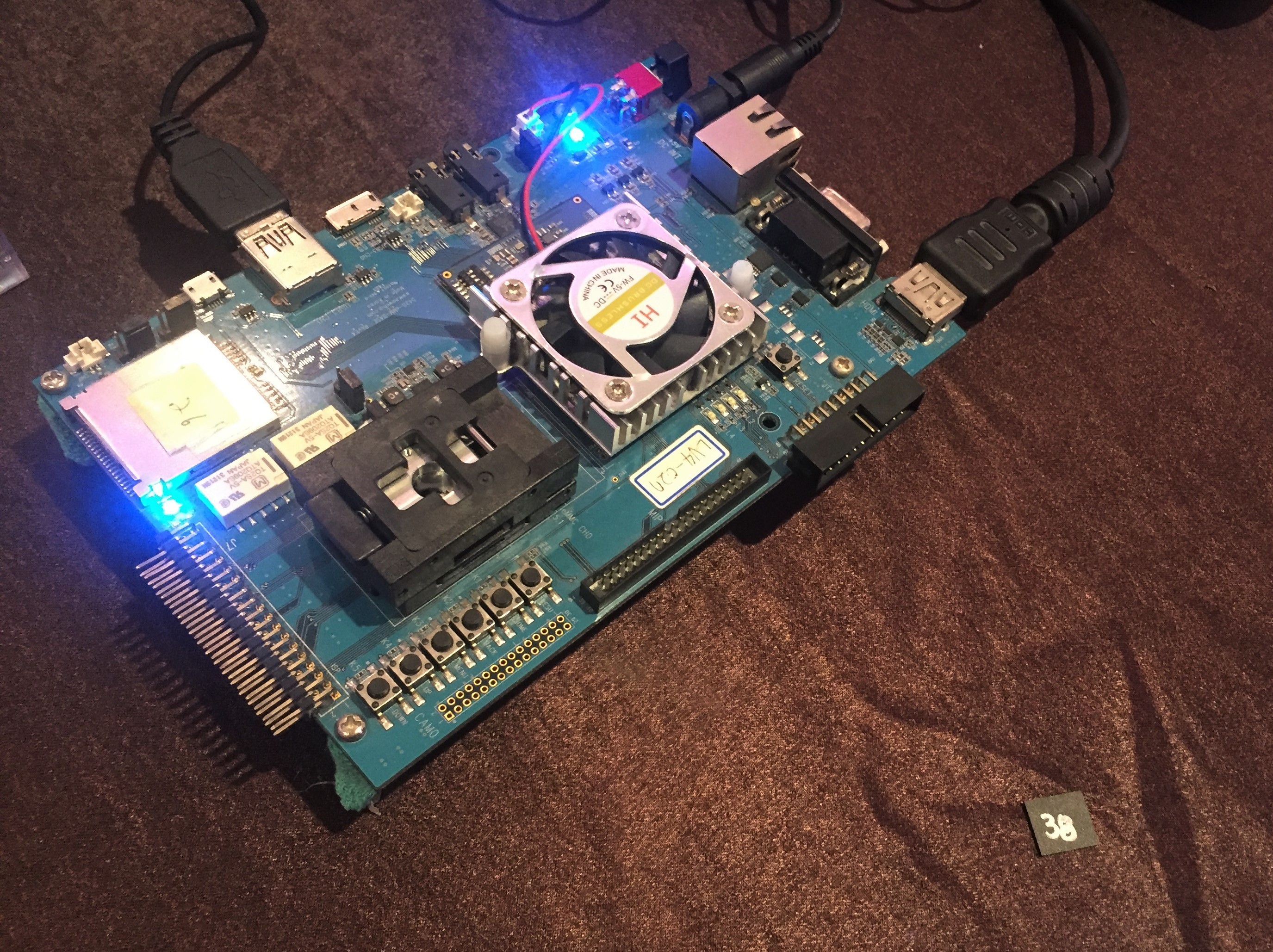
64GB SD card made with ARK core
Vice President Lee cited customized CPU core technical support as an advantage of the ARK core. The company designs and provides platforms according to the user's environment and supports FPGA design, chip fabrication, and evaluation and testing. The JUNO S0 core provides source code, compiler, and development environment free of charge when used for non-commercial purposes. The Diet-UNO platform is also free. ADchips plans to develop CPU cores at 400MHz to 1GHz levels and said it will continue compiler support activities.
Developing professional healthcare with Tiny ARK core
Hancom GMD developed a low-power healthcare SoC using the Tiny ARK core and said it has reached mass production stage. Among existing smartwatches, inexpensive products show error rates up to 30%, while expensive ones show less than 5% error rates. A Hancom GMD official said, "For professional-grade healthcare, 'delivering biological signals with less than 5% error rate' was important," and said they focused on ADC precision, package size, and current consumption. In addition, they secured competitiveness by reducing license costs with the ARK core.
Advantages include ▲using multiple registers compared to equivalent products resulting in lower memory access ratio, ▲equipped with cache controller for wider utilization, ▲low gate count resulting in lower proportion in the same process. Additionally, they stated, "With the company's headquarters located domestically, technical support is available within one hour of a phone call, and the core is provided in DB format allowing pre-verification, which was convenient."
On the other hand, they noted that the compile level is still insufficient. They said infrastructure compared to foreign products is lacking, and even guide manuals are unsatisfactory, requesting continuous assistance. They mentioned that when using the compiler, tool download speed is slow and download options must be entered individually for each board, which was inconvenient.
Vice President Lee said, "As we proceeded with this project, we made improvements based on customer requests," mentioning securing AXI bus bridge IP, acquiring a compiler supporting Bit-field, securing a cache-free Tiny core platform, and improving debugging speed. "We have now accommodated fabless companies that previously only used ARM," he said.
ETRI's Aldebaran Processor 5 (AB5) complying with autonomous driving ISO26262
Aldebaran currently has developed boards including SoC AB3 and AB5 developed jointly with major domestic companies, FPGA AB-FVU developed to support deep learning functions, as well as AB-F7 and AB-F7A.
ETRI's senior researcher Kwon Young-su countered concerns saying "The size is large," and "support stops when research is finished," asserting "the size is technically equivalent to Cortex A6, A9, or M7 among existing ARM series, and we have continued support until technology realization."
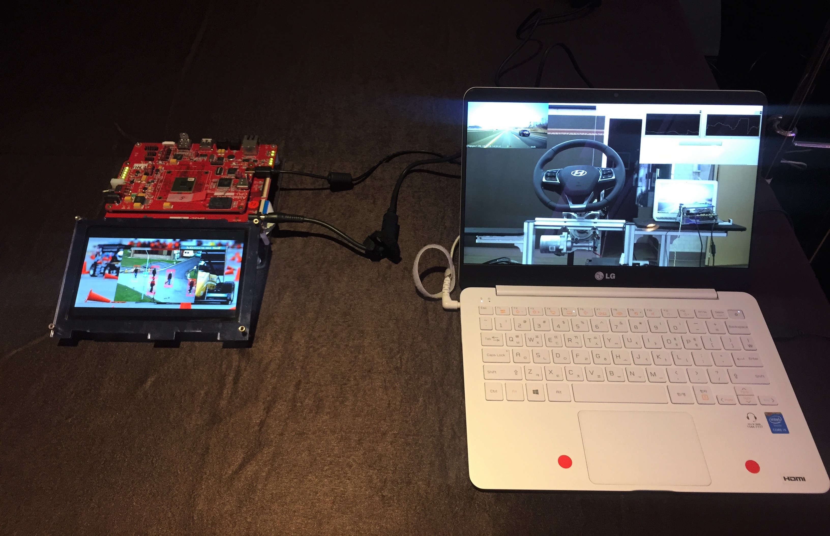
He introduced the AB5 core developed in December last year, complying with the Autonomous Vehicle Safety Level Standard (SAE J3016) L2-3 level. As an upgraded version of AB3, it complies with ISO26262. Compared to existing versions, the number of cores increased from 4 to 9, and power consumption can be minimized to around 1 watt. With a chip size of 7×8mm, when packaged, the ECU board can be manufactured around 10cm, allowing easy mounting inside vehicles.
Senior researcher Kwon Young-su said, "ARM core does not allow RTA modification, so we adopted an entire block ISP boosting engine method," and "we made efforts to maintain stability to the level of CAN controller among microchips."
At the demo booth, an ADAS application processor reproduced with AB3 was displayed. Senior researcher Shin Kyung-sun said, "Currently the algorithm only recognizes pedestrians and adjusts handle angles when drifting from lanes, and a mid-to-long-term goal is to develop processors handling artificial intelligence for future SoCs."
Tampering prevention and security-enhanced smart meter SoC
S&A developed a tampering prevention and security-enhanced smart meter SoC applying Aldebaran CPU. The official cited advantages of the Aldebaran core as ▲high performance equivalent to Cortex-A9 grade ▲various peripheral support ▲CPU cache 32x8K allowing fast perceived speed even with slow memory devices like NOR Flash ▲MMU memory structure enabling easy access to virtual and physical addresses ▲users can specify whether to use cache, allowing direct access to increase response speed.
"Besides fast support from domestic development, compiler/debugger/firmware upload is provided within virtual machines, requiring no separate setup, which is a considerable economic advantage for companies," they said.
On the downside, they noted that Windows development environment is not available as in the previous year, making development in unfamiliar Linux environment difficult. "Initial access must be easy for IC development promotion, but the unfamiliar system caused delays," they said. Additionally, due to the absence of integrated development environment (IDE), they experienced inconvenience running source editing, compilation, and debugger separately, and uploading separately.
KETI: "Realizing lightweighting tailored to customer requirements"
The Korea Electronics Technology Institute focused on MCU development based on hardware capable of efficiently calculating intelligent algorithms, following previous projects. With IoT technology advancement, they determined that high-performance CPUs required for high-speed iterative calculations are not suitable for intelligent algorithm configuration and efficient calculation.
A KETI researcher said, "Continuous customer requirements for MENSA were 'lightweighting,'" and reflecting these demands, "we developed the TINY MENSA core at approximately 65,000 gate count by removing MMU and cache."
Voice recognition SoC with built-in ultrasonic data communication capability
Emtec Vision developed a voice recognition SoC with built-in ultrasonic data communication capability using the MENSA core. This enables 93% recognition rate and data communication at distances up to 5 meters maximum. In the first-phase project, MENSA was verified on FPGA, and a 24 kHz delta-sigma ADC was designed. The current second-phase project is in the stage of fabricating and verifying SoC-based prototypes.
The development environment provides IDE with GCC-based Linux Eclipse and debug interface with target via Open OCD. Advantages include ▲equipped with interrupt controller like Cortex M, eliminating need for external INTC, ▲supporting various core options such as I/D cache, MMU, FPU ▲fast support and license cost savings as advantages of domestic CPU. An Emtec Vision researcher also raised voice for Windows IDE support and improvement of guide documentation during initial market entry.
Comments
Related news

Will domestic production of image processing processors secure competitiveness in autonomous vehicles?
The Aldebaran processor is a purely domestic Korean CPU that does not use ARM cores and is capable of supporting high-resolution video processing, offering bright prospects for the realization of autonomous vehicles in the future. The new Aldebaran processor, AB-TS3, is equipped with a quad-core capable of 4K video processing, an H.265 (HEVC) encoder, and VD/PD/LD engines.
2015.10.12by 신윤오 기자
[CPU Planning ①] How Much Do You Know About Domestic CPU Cores?
The domestic CPU core roadshow introduced Core-A from Dynarit Systems, emCore from A.D. Chips, Aldebaran from the Electronics and Telecommunications Research Institute (ETRI), and MENSA core from the Korea Electronics Technology Institute (KETI). SoC development cases utilizing these cores were demonstrated by participating companies, including Believe Micron's location-based wireless communication SoC for digital transceivers (applying Core-A), MCS Logic's wireless speaker SoC with embedded USB DAC (applying emCore), and Unmanned Solution's small mobile robot platform control SoC (applying Aldebaran).
2016.05.10by 신윤오 기자
[Reporter's Notebook] Will the application of domestic cores be a money-maker or a bomb?
AD Chips selected 'CPU' with high technical difficulty as a breakthrough for survival as a venture company in 1998. This was because at that time, there was no readily usable CPU (Central Processing Unit) core available domestically. The company believed that developing a CPU core, which is essential for SoC design, would create a competitive moat that even large corporations could not easily catch up to. Lee Hee, Vice President of AD Chips, stated, "As a person who studied electronics engineering, I chose CPU technology as a legacy to leave behind and as technology to pass on to future generations." However, the challenge was technology. In a situation where overseas companies possessed strong leading-edge technologies, the company needed to secure differentiation and competitiveness. It also had to avoid intellectual property disputes with companies such as ARM, Intel, and IBM. The technology that emerged from these efforts became EISC (Extended Instruction Set Code) ISA, which forms the foundation of Korea's homegrown CPU core, emCORE.
2016.05.10by 신윤오 기자

Intel Unveils Next-Generation 'Core Ultra Series 3' and vPro Platform for Enterprise PCs
Intel has officially unveiled the "Intel Core Ultra Series 3" for next-generation enterprise PCs and the latest vPro platform, addressing a wide range of demands from enterprise notebooks to high-performance workstations.
2026.03.26by 배종인 기자

ROHM Launches ESD Protection Diode Compatible with High-Speed Interfaces of 10Gbps or Higher
Semiconductor specialist ROHM has developed the 'RESDxVx series' of ESD (electrostatic discharge) protection diodes capable of responding to next-generation high-speed data communication environments exceeding 10Gbps, simultaneously enhancing both signal quality maintenance required in high-speed interfaces and IC protection performance.
2026.03.26by 배종인 기자











