


Promoting collaboration between industry, academia, and research institutes to develop next-generation core technologies for system semiconductors and cultivate high-quality human resources.
 Published2019.05.09 15:56
Five universities are establishing semiconductor convergence majors.
| Facility equipment upgrade and operating cost support
To secure the mid- to long-term competitiveness of the domestic system semiconductor industry, the development of future core technologies and the training of convergence experts are being promoted.
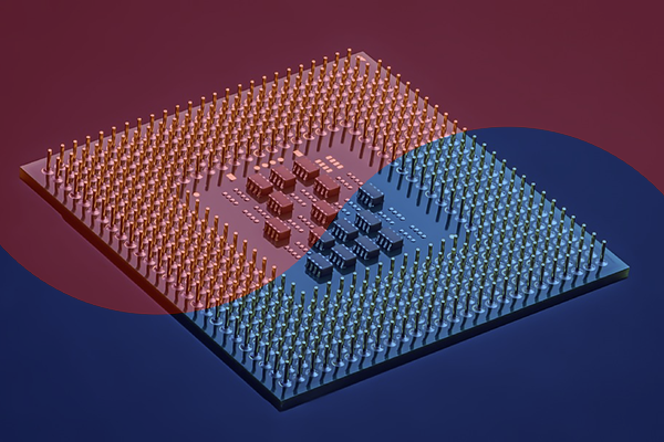
The Ministry of Science and ICT announced on the 9th that as a follow-up measure to the “System Semiconductor Vision and Strategy” announced together with the Ministry of Trade, Industry and Energy, it will pursue tasks such as developing new concept semiconductor device source technologies and integration/verification technologies, and training advanced experts in convergence system semiconductors.
At the end of April, the government presented its “System Semiconductor Vision and Strategy” with a vision to expand the domestic fabless industry’s global market share to 10% by 2030, along with strategies such as ▲strengthening demand creation and support for each stage of growth for domestic fabless companies ▲creating an ecosystem for the shared growth of fabless and foundries ▲large-scale human resource development through public-private joint projects and securing next-generation semiconductor technology.
The Ministry of Science and ICT is working to develop core technologies for new concept devices, foster advanced professionals in system semiconductor convergence, support fabless companies using public nanofabs, establish research bases based on public-private collaboration, and strengthen the role of government-funded research institutes as semiconductor research platforms, thereby enabling Korea to leap beyond the global leader in memory semiconductors to become a comprehensive semiconductor powerhouse.We plan to focus particularly on mid- to long-term investments in people and technology to enable this.
By strengthening the connection between 5G+ core industry services and domestic system semiconductor companies, the world's first 5G commercialization will be used as an opportunity to create new demand for the domestic fabless industry, while also promoting the provision of essential semiconductor design programs and support for strengthening technological capabilities.
Development of next-generation semiconductor core technologies
Through the "Next-Generation Intelligent Semiconductor Technology Development Project," which passed the preliminary feasibility study at the end of April, approximately 240 billion won will be invested over the next 10 years to develop new semiconductor element source technologies that can change the paradigm of the semiconductor industry.
In order to overcome the limitations of miniaturization that have been the paradigm of semiconductor technology development and to develop new ultra-high-performance, ultra-low-power devices, we plan to develop new device source technologies such as ultra-low-voltage and microcurrent control devices, 3D devices, and brain-mimicking devices. At the same time, we plan to further strengthen the early commercialization of new devices and industry-academia collaboration and linkages by developing new device integration and verification technologies that go beyond unit-device research.
We also plan to support the development of innovative basic technologies for devices such as bio-fusion future semiconductors that utilize DNA structures.
Training of convergence experts in the system semiconductor field
To address the chronic shortage of top-tier system semiconductor design personnel, the program will also foster master's and doctoral-level system semiconductor convergence specialists who possess not only practical skills but also in-depth understanding of manufacturing in general, including components and processes, as well as system semiconductor application fields such as bio, future automobiles, and robotics.
A consortium of about 5 universities will be selected, and each consortium will be supported with approximately 10 billion won over the next 6 years. Each consortium formed with semiconductor-related universities will major in system semiconductor convergence.The program will produce advanced design professionals with problem-solving skills through new programs (processes), industry-academia collaboration research, and capstone projects (system semiconductor design in specialized fields based on corporate demand during the training period).
Supporting fabless companies using public nanofabs
We will strengthen support for small and medium-sized fabless companies, focusing on public nanofabs capable of supporting semiconductor manufacturing in Daejeon, Suwon, and Pohang.
First, we will enhance foundry service support by providing semiconductor design support tools (Process Design Kit; PDK) to support multi-project wafer (MPW) services.
In addition, by linking with the Ministry of SMEs and Startups' research equipment utilization support project, etc., we plan to significantly reduce the burden of utilizing public nanofabs for small and medium-sized fabless startups by around 70%, thereby increasing accessibility to nanofabs.
Establishing a research hub for industry-academia collaboration and fostering leading research groups
In conjunction with recent large-scale investments by major semiconductor companies, a research base will be established based on joint investment by large companies and the government.
SK Hynix announced plans to invest 120 trillion won to create a semiconductor cluster in Yongin, Gyeonggi Province, and Samsung Electronics announced plans to invest 133 trillion won to enhance the competitiveness of system semiconductors, including foundries.
The Ministry of Science and ICT also plans to foster leading research groups through large-scale group research that combines the capabilities of research and industry, such as joint use of semiconductor research and mass production facilities of large corporations and joint research to solve corporate challenges. Specific measures will be prepared by the end of this year after consultation with relevant large corporations.
Strengthening the role of government-funded research institutes as semiconductor research platforms
A consultative body comprised of government-funded research institutes with excellent research personnel and research infrastructure, such as KIST, ETRI, Korea Institute of Standards and Technology, Electronics and Telecommunications Research Institute, and Korea Institute of Industrial Technology, will be formed and launched this month.
To successfully promote the government's large-scale semiconductor technology development project, the council plans to strengthen its role as a platform for innovation in the semiconductor research ecosystem, including linking core and applied technologies, as well as supporting the early commercialization of excellent technologies and fabless startups through research institutes' infrastructure.
Meanwhile, Vice Minister of Science and ICT Moon Mi-ok will visit the Daegu Gyeongbuk Institute of Science and Technology (DGIST) on the 10th to discuss specific policies and projects to foster the people and technologies that will support Korea's leap forward as a comprehensive semiconductor powerhouse. She will also gather input from industry, academia, and research representatives. This will be the second on-site meeting on semiconductors by the MOST, following a meeting with fabless companies on the 8th.
The Ministry of Science and ICT plans to continuously strive to ensure the smooth implementation of the “System Semiconductor Vision and Strategy” and the practical application of specific implementation plans through continuous collection of opinions from the field.
Comments
Related news
"Becoming a Comprehensive Semiconductor Powerhouse by 2030" Government Announces Fostering System Semiconductor Ecosystem
As the Fourth Industrial Revolution era unfolds, semiconductor demand is expanding from PCs and mobile devices across all industries including automobiles, robotics, energy, and biotechnology, driving increased demand for system semiconductors. However, Korea has been hindered by a shortage of specialized personnel, insufficient ecosystem competitiveness, and poor linkage with demand industries, resulting in a low market share of 3.1% as of 2018. Additionally, technological capabilities stand at 80% of the U.S. level, and only one domestic company is among the top 50 global fabless firms. To overcome these challenges, the government has established five key measures to leap forward as a comprehensive semiconductor powerhouse by 2030. While related measures existed in the past, they were insufficient in fostering an ecosystem and fell short of meeting corporate demands. This initiative places emphasis on creating a self-sustaining ecosystem for the system semiconductor industry.
2019.05.02by 이수민 기자

Samsung Electronics Expands and Relocates its Montreal AI Lab to Focus on AI Research Applicable to Next-Generation System Semiconductors
Samsung Electronics is expanding and relocating its Comprehensive Technology Institute Montreal AI Lab to a building at the Mila Institute located in Montreal, Canada, thereby strengthening its research in the future AI field. The Mila Institute is a world-leading deep learning research institution where Professor Yoshua Bengio, one of the world's top three scholars in deep learning, collaborates with researchers from the University of Montreal and McGill University, as well as AI developers from global companies. With this move, Samsung Electronics becomes the first Korean company to establish a presence in the Mila Institute building. Concurrent with this expansion and relocation, Samsung Electronics has recruited Simon Lacoste, a professor at the University of Montreal affiliated with the Mila Institute, and appointed him as the head of the Montreal AI Lab.
2019.05.02by 이수민 기자
The IIoT Environment of the 5G Era That Edge Computing Will Transform
In 2017, Gartner selected "Cloud to the Edge" as one of the top 10 strategic technology trends for 2018. In 2018, the Information and Communications Technology Promotion Center also cited "the growth of edge computing and AI semiconductors due to the proliferation of IoT" as one of the top 10 ICT issues for 2019. Why exactly is edge computing such an issue? Smart devices are increasing day by day. Until now, all data generated from devices has been sent to the cloud for processing. However, recognizing this process as inefficient, movements are emerging in various places to process data at the location where it is generated or in nearby locations. This attempt to perform computing at the network edge and process critical data close to real-time is referred to as edge computing.
2019.05.08by 이수민 기자

Intel Unveils Next-Generation 'Core Ultra Series 3' and vPro Platform for Enterprise PCs
Intel has officially unveiled the "Intel Core Ultra Series 3" for next-generation enterprise PCs and the latest vPro platform, addressing a wide range of demands from enterprise notebooks to high-performance workstations.
2026.03.26by 배종인 기자

ROHM Launches ESD Protection Diode Compatible with High-Speed Interfaces of 10Gbps or Higher
Semiconductor specialist ROHM has developed the 'RESDxVx series' of ESD (electrostatic discharge) protection diodes capable of responding to next-generation high-speed data communication environments exceeding 10Gbps, simultaneously enhancing both signal quality maintenance required in high-speed interfaces and IC protection performance.
2026.03.26by 배종인 기자











