



OLED displays for VR and AR are manufactured on glass substrates.
 Published2019.11.25 09:01
1,867 PPI achieved on VR/AR displays
100% reliance on Japan, large-area production possible without FMM
The displays of VR and AR devices are darker and less sharp than those of TVs and smartphones, causing a significant number of users to struggle with prolonged immersion.
To achieve vivid image quality, the pixel density, or PPI (Pixels Per Inch), must be increased to a level where individual pixels cannot be distinguished by human vision, and it must improve proportionally as the display is placed closer to the eye.
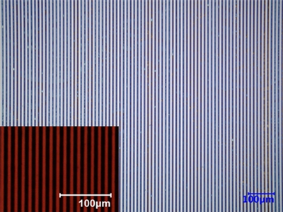
Device pattern and emission image (Photo = KITECH)
The Korea Institute of Industrial Technology (KITECH) announced on the 19th that it has developed a process technology capable of manufacturing OLED pixels for VR and AR using the RGB method on a glass substrate, and has succeeded in achieving a resolution of 1,867 PPI.
Generally, while 4K UHD TVs require 100 to 200 PPI and smartphones require 500 PPI, VR/AR devices worn close to the eyes must meet at least 1,800 PPI.
OLED pixels are manufactured by depositing organic materials at regular intervals on a substrate and are broadly classified into RGB and WOLED methods.
The RGB method, which deposits red, green, and blue organic materials in sequence, makes it difficult to develop processes for increasing pixel density compared to the WOLED method, which applies color filters to white OLEDs, but it offers superior brightness and power efficiency.
High-resolution display substrate materials for VR and AR are divided into glass and silicon wafers; while glass substrates are at a disadvantage compared to silicon wafer substrates for achieving high resolution, they are advantageous for manufacturing large displays due to their lower production costs.
A research team led by Dr. Kwan-Hyun Cho of the Micro-Nano Process Group developed a high-resolution OLED display manufacturing process suitable for VR and AR by leveraging the advantages of both RGB and glass substrate methods.
The core of this source technology lies in a special container composed of multiple microchannels that can hold the OLED solution at intervals of 13.6㎛ (micrometers), a selective surface treatment technique that causes the solution to adhere only within the channels, and a photothermal conversion layer that absorbs light and converts it into heat.
The principle is that a glass substrate is placed on a special container, and then a xenon flash lamp that emits a strong light instantaneously is activated underneath, causing the photothermal conversion layer inside the special container to rapidly vaporize the OLED solution with heat of over 300°C and deposit it onto the substrate at predetermined intervals.
The key advantage of this technology is that it enables the low-cost production of high-resolution OLED displays for VR and AR on glass substrates that can be scaled up. This facilitates mass production, and for users, it offers a wider viewing angle, enhancing immersion and alleviating dizziness.
In addition, since a photothermal conversion layer is utilized when depositing organic materials onto a substrate, there is no need to use a Fine-Metal Mask (FMM), which is an essential material for conventional RGB deposition processes. FMM, which is 100% exclusively produced in Japan, is a thin steel plate with densely packed fine holes that helps organic materials be deposited at specific locations on a substrate.
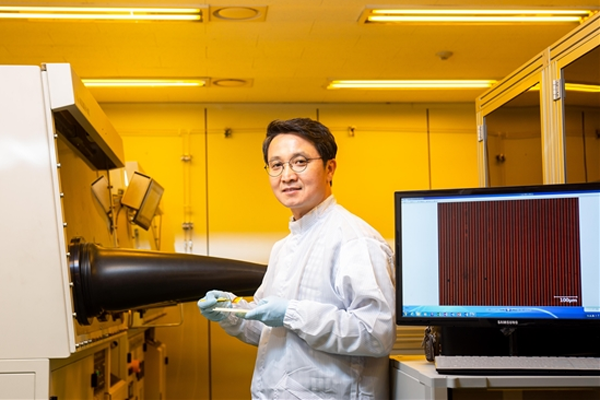
Dr. Cho Kwan-hyun said, “We were able to deposit RGB OLEDs on glass substrates under optimal conditions by leveraging our experience and know-how from previous photothermal conversion research,” adding, “We plan to increase the resolution to 2,000 to 3,000 PPI by utilizing microelectromechanical systems (MEMS) processes capable of producing devices several micrometers in size.”
Comments
Related news
PTC supplies Vuforia, its AR development platform, to Samsung Electronics, to be used in Samsung's HA AR app.
PTC supplied its AR development platform Vuforia to Samsung Electronics' Home Appliances Business Division. Samsung Electronics launched Samsung HA AR, an augmented reality mobile application based on Vuforia. Samsung HA AR is an application that enables consumers to view and intuitively understand innovative technologies applied to Samsung Electronics' major home appliance products through augmented reality. Consumers can visit Samsung Digital Plaza stores in Korea or global retail outlets and use the application installed on tablets to verify product features and benefits through 3D AR.
2019.05.14by 이수민 기자
What is the core of the top 10 strategic technology trends of '20? "Humans and Space"
Gartner, focusing on human-centric smart spaces, has announced the top 10 strategic technology trends for 2020 that enterprises should pay attention to. The top 10 strategic technology trends for 2020 consist of two categories of technologies. These are emerging technologies with innovative potential demonstrating broader impact and use cases as they move beyond their early stages, as well as technologies exhibiting rapid growth and expected to reach their peak within the next five years. Gartner's top 10 strategic technology trends for 2020 are hyperautomation, multiexperience, democratization of expertise, human augmentation, transparency and traceability, autonomous edge, distributed cloud, autonomous things, practical blockchain, and AI security.
2019.10.26by 이수민 기자
5G-exclusive AR glasses equipped with spatial recognition and mirroring technology
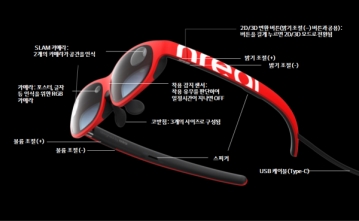
LG U+ and nreal have made an exclusive domestic debut of the 5G-dedicated AR glasses 'Nreal Light'. The device is designed with lightweight characteristics of merely 88g and a wearable design suitable for everyday use, while incorporating high-definition OLED and 100-inch large-screen mirroring technology. LG U+, which will operate an experience zone from the 21st, plans to conduct pilot services through the first quarter of 2020 and commercialize the product in the first half of 2020.
2019.11.21by 최인영 기자

Intel Unveils Next-Generation 'Core Ultra Series 3' and vPro Platform for Enterprise PCs
Intel has officially unveiled the "Intel Core Ultra Series 3" for next-generation enterprise PCs and the latest vPro platform, addressing a wide range of demands from enterprise notebooks to high-performance workstations.
2026.03.26by 배종인 기자

ROHM Launches ESD Protection Diode Compatible with High-Speed Interfaces of 10Gbps or Higher
Semiconductor specialist ROHM has developed the 'RESDxVx series' of ESD (electrostatic discharge) protection diodes capable of responding to next-generation high-speed data communication environments exceeding 10Gbps, simultaneously enhancing both signal quality maintenance required in high-speed interfaces and IC protection performance.
2026.03.26by 배종인 기자











