



ToF Utilization Increases Significantly… ST Ships 1 Billion ToF Modules
 Published2019.12.02 11:01
Applied to 150 types of smartphones
The adoption rate of ToF sensors in smartphones appears to be increasing dramatically.
(Image=STMicroelectronics)
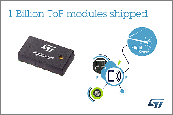
STMicroelectronics announced on November 29 that it shipped its 1 billionth ToF module.
Time of Flight (ToF) is a technology that calculates distance by measuring the time it takes for a light source sent toward an object to reflect back. When combined with a camera, it can represent objects in three dimensions.
The process of recognizing objects in 3D is simple and is not affected by external light interference, resulting in a high recognition rate even outdoors. It has a fast response speed, making it highly useful.
ToF modules equipped with ST's SPAD (Single Photon Avalanche Diode) sensor technology are being produced at ST's 300nm front-end wafer fab located in Croll, France.
The final module, integrating the optical components, SAPD sensors, and VCSELs (Vertical Cavity Surface Emission Lasers) required to realize the product's performance, undergoes assembly and testing at ST's back-end facilities.
"ST's ToF modules are currently used in over 150 types of smartphones," said Eric Aussedat, Head of the ST Imaging Subgroup. "Recently, we added high-resolution 3D depth sensing capabilities to enable applications utilizing advanced proximity sensing, human presence detection, and laser autofocus."
Currently, ST is mass-producing the VL6180, VL53L0, and VL53L1 product families for the consumer, personal computer, and industrial markets.
Comments
Related news
LG Electronics to Include Infineon ToF Sensor in Its 2019 Strategic Smartphone, the G8
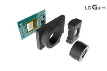
LG Electronics will equip its strategic smartphone new product LG G8 ThinQ with an advanced 3D sensor based on time-of-flight distance measurement technology. Time-of-flight distance measurement is a technology that calculates distance by measuring the time it takes for light emitted toward an object to reflect and return. When combined with a camera, it enables three-dimensional representation of objects. In particular, the process of recognizing objects in 3D is simple and unaffected by external light interference, providing excellent recognition rates even outdoors, which is advantageous for implementing AR and VR.
2019.02.11by 이수민 기자

ams Launches Infrared Illuminator Optimized for 3D Optical Sensing in Mobile Devices
ams has launched the MERANO-PD, an infrared laser illumination module that provides uniform lighting output for mobile 3D sensing applications such as facial recognition. The MERANO-PD features high power efficiency and is compatible with state-of-the-art 3D sensing technologies including ToF and structured light (SL) techniques. The MERANO-PD can be utilized in a wide range of applications including facial recognition, augmented reality, 3D object scanning and 3D image rendering, as well as various applications in industrial and automotive fields.
2019.02.27by 이수민 기자
eGaN FETs for LiDAR - Getting the Most Out of Laser Drivers Theory
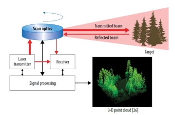
Lidar is a form of radar that generates electromagnetic waves in a broad spectrum. Over the past several years, Time-of-Flight (TOF) distance measurement, one specific form of lidar, has been widely adopted. When a laser is used as the optical source, distance measurements can be taken even to small areas at far distances, and when used with adjustable optical devices, the distance to that point can be measured and a three-dimensional map of the object can be implemented.
2019.09.09by 명세환 기자

Intel Unveils Next-Generation 'Core Ultra Series 3' and vPro Platform for Enterprise PCs
Intel has officially unveiled the "Intel Core Ultra Series 3" for next-generation enterprise PCs and the latest vPro platform, addressing a wide range of demands from enterprise notebooks to high-performance workstations.
2026.03.26by 배종인 기자

ROHM Launches ESD Protection Diode Compatible with High-Speed Interfaces of 10Gbps or Higher
Semiconductor specialist ROHM has developed the 'RESDxVx series' of ESD (electrostatic discharge) protection diodes capable of responding to next-generation high-speed data communication environments exceeding 10Gbps, simultaneously enhancing both signal quality maintenance required in high-speed interfaces and IC protection performance.
2026.03.26by 배종인 기자











