



"Electronic device form factors are becoming more diverse." IBS succeeds in synthesizing large-area single-crystal metal thin films.
 Published2020.05.28 17:05
Successful diversification of high-performance two-dimensional material synthesis materials
A research team led by Professor Feng Ding (a distinguished professor at UNIST) and group leader of the Center for Multidimensional Carbon Materials at the Institute for Basic Science (IBS), together with researchers from China and Switzerland, has succeeded in diversifying the surface pattern of a metal substrate for the synthesis of high-performance two-dimensional materials such as graphene.
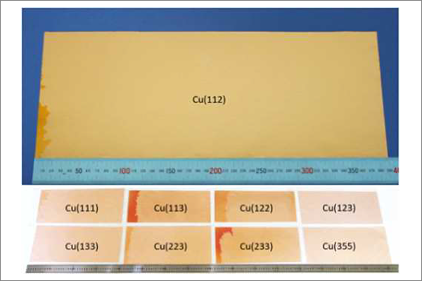
Large-area single-crystal copper thin film [Image = IBS]
Two-dimensional single-crystal materials, characterized by a regular arrangement and orientation of atoms, exhibit excellent thermal and electrical conductivity, making them suitable for use in high-performance electronic devices. However, the limited variety of single-crystal metal thin-film patterns required for the synthesis of two-dimensional single-crystal materials has been a challenge. This research synthesized a large-area (39×21㎠) single-crystal metal thin-film with approximately 30 different surface patterns.
The joint research team published a paper in Nature last May proving that the metal substrate used in material manufacturing holds the key to large-area single-crystal material production. They found that the orientation of the synthesized material varies depending on the substrate's Miller index (an index that describes the pattern of the metal substrate).
This study presents a method for synthesizing metal substrates with various Miller indices. First, a copper single crystal was cut to obtain fragments (seeds) with the desired pattern. The surface pattern varies depending on the direction in which the crystal is cut, much like the marbling of beef.
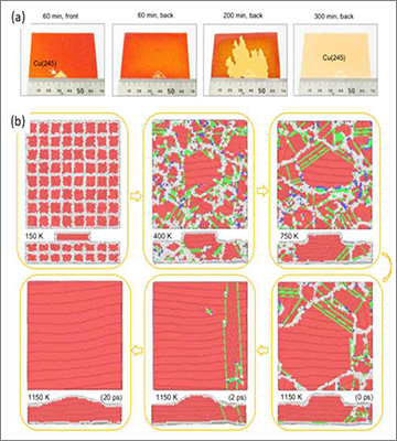
Seed growth process of copper thin films [Figure = IBS]
The fragments were then attached to a copper polycrystal and annealed for several hours at a high temperature (1020°C), close to its melting point. During this process, the crystals surrounding the fragment rearranged themselves into a pattern that mirrored the fragment's shape, gradually expanding over a wider area. Ultimately, the film transformed into a single crystal with a consistent pattern across the entire film.
Utilizing the developed technology, large-scale synthesis of metal thin films with diverse surface patterns is possible. With the expanded range of substrate options, selecting the appropriate substrate and controlling the orientation of the desired material is expected to enable the synthesis of high-performance two-dimensional materials with desired properties. For example, it is possible to manufacture substrates that can be folded or bent and used in foldable phones.
The research team expects that various metals, including the copper and nickel used in this study, can be manufactured in the form of large-area single-crystal metal thin films.
“The production of large-area single-crystal metal thin films with various crystal planes has been a long-standing goal in the field of materials science,” said Feng Ding, IBS group leader. “The large-area single-crystal metal thin films synthesized through this research can be used in various fields, such as as templates for the synthesis of various single-crystal two-dimensional materials and as catalysts that selectively induce only specific chemical reactions.”
The Ministry of Science and ICT and the IBS announced that the results of this study were published in the online edition of Nature (IF 43.070) at 00:00 on May 28, Korean time.
Comments
Related news

2021 Budget Announcement for Small Business and Big 3 Sectors, Focusing Investment on Semiconductors and New Materials
The Ministry of Science and ICT deliberated and approved five agendas, including the government's research and development investment direction for the materials, parts, and equipment (MPE) sector in 2021, which contains field-specific support priorities for semiconductors and displays, as well as investment directions for the BIG3 sectors including system semiconductors, future vehicle core components, and biohealth materials. Medium to long-term customized support and the establishment of industry-academic-research collaboration systems will be promoted.
2020.03.17by 최인영 기자

Special Measures Act to Strengthen Competitiveness of Materials, Parts, and Equipment to Take Effect on the 1st of Next Month
The Special Measures Act for Strengthening Competitiveness in the Materials, Parts, and Equipment Industry will be comprehensively reorganized for the first time in approximately 20 years since its last amendment and will take effect on April 1st. The Ministry of Industry plans to convert the special law, which was scheduled to sunset in 2021, into a permanent law and will promote the establishment of inter-company cooperation models and rent reduction for resident companies to strengthen industry-oriented competitiveness.
2020.03.24by 최인영 기자
Launch of a project to discover and foster startups in the materials, components, and equipment sectors.
The Ministry of SMEs and Startups announced that it will launch the project to discover and nurture 100 parts, materials, and equipment (SME) startups starting from the 6th. This project will focus on discovering and fostering startups that are highly relevant to future emerging industries and capable of addressing 135 technology needs in the parts, materials, and equipment sector submitted by large enterprises and others.
2020.04.06by 이수민 기자
ESP32 Development Environment Selection and GPS Application Implementation
The ESP32 is a microcontroller that integrates Wi-Fi, Bluetooth, 12-bit ADC, capacitive touch, PWM, DAC, and UART in a single SoC. However, the abundance of features does not by itself solve the designer's problems. The real challenges lie in selecting the appropriate development environment, determining which pins can be used and which must be avoided, and converting raw data from modules into usable information. This document addresses ESP32 peripheral constraints (ADC2 and Wi-Fi coexistence limitation, UART1 occupancy, ADC non-linear regions), the trade-offs between Arduino IDE and ESP-IDF, and the process from connecting NEO-6M/NEO-M8N GPS modules to UART2, parsing NMEA sentences, and visualizing routes in Google Earth, all organized based on documented references.
2026.10.12by 편집부
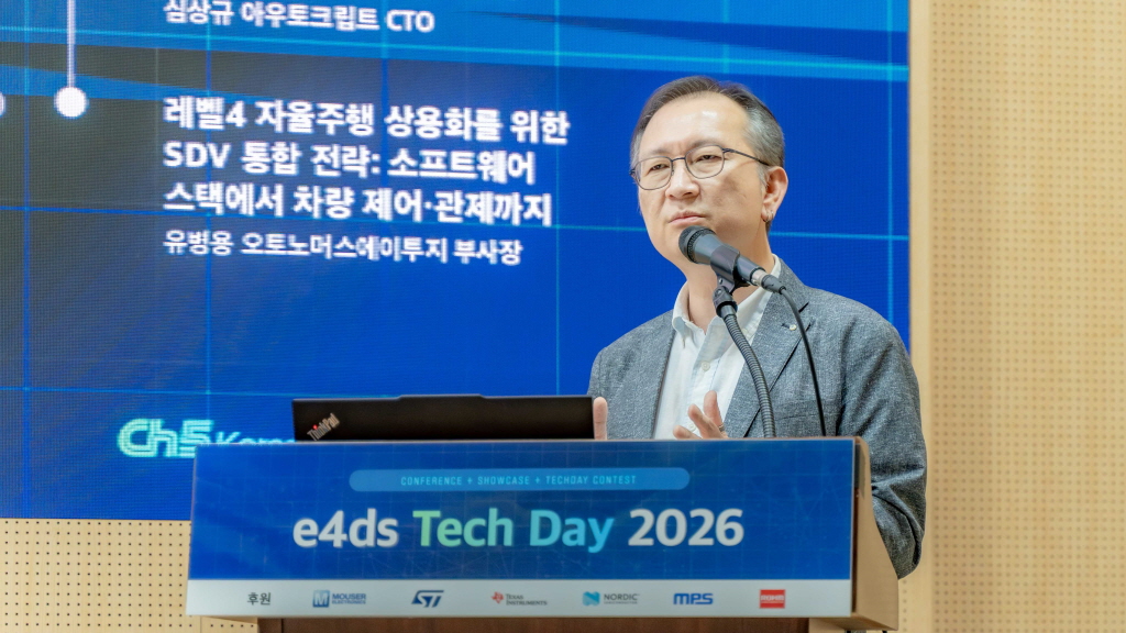
[e4ds Tech Day 2026 ⑨] Sim Sang-gyu, Autocrypt CTO: "In the Physical AI Era, Automotive Security Must Extend Beyond the Vehicle"
At e4ds Tech Day 2026, Sim Sang-gyu, CTO of Autocrypt, explained automotive cybersecurity strategies in the era of Physical AI and SDV (Software-Defined Vehicle). Automobiles are evolving as part of an ecosystem connected to AI, cloud, chargers, IoT, and robots, and he emphasized that the scope of security must expand beyond the vehicle interior to the entire connected environment. In particular, AI model tampering, adversarial attacks, OTA updates, and EV charger hacking were identified as major threats. He explained that response measures require zero trust, AI model integrity protection, intrusion detection, Security by Design and Default, and full lifecycle security management, and that proactive security system establishment beyond regulatory compliance is critical for securing future mobility competitiveness.
2026.10.12by 배종인 기자











