


Will the 12-inch wafer-based micro-parts testbed yield results?
 Published2020.08.13 09:41
Inspection of the status of semiconductor small, medium, and large-scale test bed construction
Small and Medium Businesses Share COVID-19 Technology Commercialization Results
On the 11th, Minister of Science and ICT Choi Ki-young visited the site of the 12-inch semiconductor materials, components, and equipment localization support test bed being built at the Nano Comprehensive Technology Institute (Nano Comprehensive Technology Institute) to inspect the progress and held a meeting to promote the test bed.
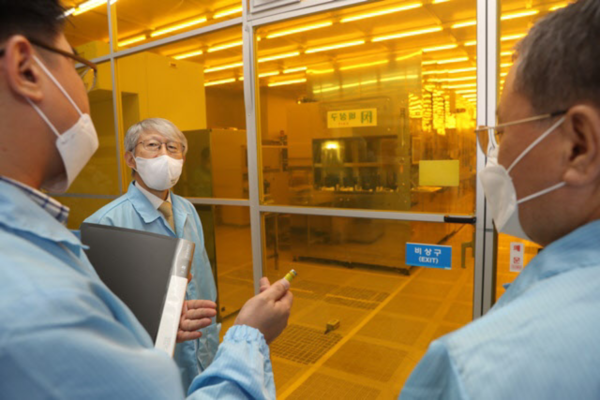
[Photo = Ministry of Science and ICT]
The testbed provides a production environment similar to that of large-scale mass production facilities, supporting testing and performance evaluation of materials, components, and equipment from small and medium-sized enterprises (SMEs). Since the second half of last year, the Ministry of Science and ICT has been promoting the introduction of 10 core pieces of equipment required for the testbed.
The construction of a 12-inch wafer-based semiconductor test bed at Nano Jong-giwon will cost 45 billion won (38.5 billion won for equipment construction, 4.3 billion won for facilities, and 2.2 billion won for process development) from 2019 to 2022.
A dedicated testbed cleanroom was built in June, and an ArF immersion exposure machine and track were delivered in July. The remaining equipment (eight units) is scheduled to be delivered within the year. We plan to provide pilot services simultaneously with equipment installation and improve the quality of services through process advancement.
The meeting held after the on-site inspection was attended by many people involved in the semiconductor industry, including small and medium-sized enterprises in the semiconductor materials, parts, and equipment sectors, the Korea Semiconductor Industry Association, Samsung Electronics, SK Hynix, and ASML Korea, and discussed corporate suggestions for the development of the test bed and ways for mutually beneficial cooperation.
The symposium also showcased the success stories of companies that have recently leveraged the NanoCell Fab to successfully develop and commercialize technologies. These include: Truewin Co., Ltd., which produced an infrared thermal imaging sensor; TNS Co., Ltd., which produced a COVID-19 diagnostic kit; Tempus Co., Ltd., which produced a non-contact infrared thermometer; and DCT Co., Ltd., which produced a hard mask for memory semiconductors.
Minister Choi Ki-young emphasized at the meeting, “It is most important that materials and parts that have passed the test bed are purchased by actual demand companies,” and “It is important to improve the quality of the test bed service for small and medium-sized enterprises of the Nano-Generation Institute and for the end-user companies to actively approach them.”
Nano-Chonggiwon plans to strengthen cooperation with the Korea Semiconductor Industry Association to link the basic and application performance evaluation results of the test bed to the mass production evaluations of demand companies, while also pursuing overall service innovation through expansion of open equipment and usage hours, and personnel expansion.
Furthermore, to address infectious disease issues such as COVID-19, we plan to more actively pursue the development of nanobio devices through collaboration with universities, research institutes, hospitals, and companies, based on nanofab equipment and process technology.
Comments
Related news

GaN power semiconductors with high power density and low heat generation: "100% in-house development reduces price."
Power semiconductors are semiconductors that supply, control, and convert electrical power, serving as core components responsible for the operation and performance of electronic products. With the advent of the Fourth Industrial Revolution era in recent years, various advanced fields are experiencing growth. Consequently, the importance of power semiconductors capable of handling high output and high voltage is increasing further.
2020.07.28by 이수민 기자
Semiconductor packaging materials market projected to grow at an average annual rate of 3.4%.
SEMI cited the latest global semiconductor packaging materials outlook report from TechSearch, a specialized research institute for the electronics industry, and announced that the semiconductor packaging materials market size is projected to grow from $17.6 billion in 2019 to $20.8 billion in 2024, with a compound annual growth rate of 3.4%.
2020.07.29by 강정규 기자
Teledyne Announces ToF CMOS Image Sensor for 3D Sensing
Teledyne e2v has announced Hydra3D, a ToF CMOS image sensor for 3D sensing and distance measurement. The new sensor, which features a 10μm 3-tap pixel, was designed using Teledyne e2v's proprietary CMOS technology. Production is handled by Tower Semiconductor, an analog semiconductor foundry based in Israel.
2020.08.12by 강정규 기자

Intel Unveils Next-Generation 'Core Ultra Series 3' and vPro Platform for Enterprise PCs
Intel has officially unveiled the "Intel Core Ultra Series 3" for next-generation enterprise PCs and the latest vPro platform, addressing a wide range of demands from enterprise notebooks to high-performance workstations.
2026.03.26by 배종인 기자

ROHM Launches ESD Protection Diode Compatible with High-Speed Interfaces of 10Gbps or Higher
Semiconductor specialist ROHM has developed the 'RESDxVx series' of ESD (electrostatic discharge) protection diodes capable of responding to next-generation high-speed data communication environments exceeding 10Gbps, simultaneously enhancing both signal quality maintenance required in high-speed interfaces and IC protection performance.
2026.03.26by 배종인 기자











