



STMicroelectronics Launches 6kV Galvanically Isolated High-Voltage Gate Driver
 Published2020.11.09 10:31
Sink and source up to 4A of output current
STMicroelectronics (ST) announced on the 9th that it has launched the compact high-voltage gate driver, the STGAP2HS. This product supports applications that require up to 6kV of galvanic isolation between the gate drive channel and low-voltage control and interface circuits.
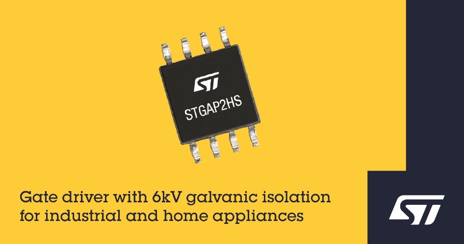
This 1200V device can sink and source up to 4A of output current, simplifying design and improving the reliability of medium- and high-power converters and power supplies, home appliance inverters, and industrial equipment such as factory automation, fans, induction heaters, welders, and UPS.
Additionally, it features dual input pins that allow designers to control signal polarity, and interlocking protection to prevent cross-conduction in the event of a controller malfunction. The inputs are compatible with CMOS/TTL logic up to 3.3 V, allowing easy interfacing with control devices. Furthermore, matching the propagation delay between low- and high-voltage sections prevents cycle distortion, minimizes energy loss, and enables high-frequency operation. CMTI is ±100 V/ns over the full -40°C to 125°C temperature range.
The STGAP2HS is available in two configurations: One configuration features separate output pins, allowing independent optimization of turn-on and turn-off times using dedicated gate resistors. The second configuration provides a single output pin and a Miller-clamp function to prevent gate spikes during high-speed commutation in half-bridge topologies. Each configuration allows designers to use N-channel MOSFETs in both high- and low-side bridge circuits, reducing external component costs.
The STGAP2HS integrates dedicated UVLO and thermal shutdown protection for both the low-voltage and high-voltage drive channels, along with overtemperature protection. This enhances reliability by preventing power switches from operating under low-efficiency or hazardous conditions. Input-to-output propagation delays of less than 75ns enable accurate pulse-width modulation (PWM) control, and a standby mode allows designers to reduce system power consumption.
Comments
Related news
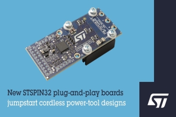
ST Launches Plug-and-Play Board to Simplify Power Tool Development
ST has launched two new plug-and-play boards to support the development of cordless power tools. The boards are powered by lithium-ion batteries up to 56V and control three-phase brushless motors. The STEVAL-PTOOL1V1 and STEVAL-PTOOL2V1 evaluation boards are based on the STSPIN32 motor control SiP (System-in-Package) and meet key requirements of power tools with compact size and low standby current. Firmware for 6-step motor commutation using Hall-Effect rotor position sensing is provided, which ensures low torque ripple and optimal power efficiency.
2020.10.29by 김동우 기자
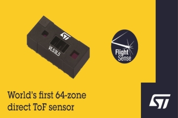
STMicroelectronics Launches All-in-One Multi-Zone Direct ToF Module
This device comprises a 940nm VCSEL light source, an SoC sensor integrating a VCSEL driver, a SPAD receive array, a low-power 32-bit MCU core, and an accelerator running sophisticated firmware. The VL53L5 is included in ST's FlightSense sensor, which is all Class 1 certified, ensuring safety from vision impairment due to laser light in consumer products.
2020.10.30by 김동우 기자

ST establishes world's first LiF plant to expand piezoelectric MEMS market
ST Microelectronics (hereinafter ST), in collaboration with the Institute of Microelectronics under A*STAR (Agency for Science, Technology and Research, Singapore, hereinafter A*STAR) and Axcelis, a leading manufacturing tool supplier from Japan, will jointly establish and operate an 8-inch (200mm) R&D line focused on piezo MEMS technology. This collaboration will strengthen ST Singapore's manufacturing process portfolio and accelerate the adoption of piezo MEMS actuators in emerging application fields. These include MEMS mirrors for smart glasses and AR headsets, LiDAR systems, PMUTs (Piezoelectric Micromachined Ultrasonic Transducers) for new medical applications, and piezo heads supporting commercial and industrial 3D printing.
2020.11.03by 김동우 기자

ESP32 Development Environment Selection and GPS Application Implementation
The ESP32 is a microcontroller that integrates Wi-Fi, Bluetooth, 12-bit ADC, capacitive touch, PWM, DAC, and UART in a single SoC. However, the abundance of features does not by itself solve the designer's problems. The real challenges lie in selecting the appropriate development environment, determining which pins can be used and which must be avoided, and converting raw data from modules into usable information. This document addresses ESP32 peripheral constraints (ADC2 and Wi-Fi coexistence limitation, UART1 occupancy, ADC non-linear regions), the trade-offs between Arduino IDE and ESP-IDF, and the process from connecting NEO-6M/NEO-M8N GPS modules to UART2, parsing NMEA sentences, and visualizing routes in Google Earth, all organized based on documented references.
2026.10.12by 편집부
MIPI CSI-2, DSI-2, C-PHY, D-PHY Test Solution Technical White Paper
The MIPI interface adopts a burst mode that transitions between low-power (LP) and high-speed (HS) states for low-power consumption, and in return, strict timing rules are imposed on state transitions. Additionally, the high-speed section operates as a packet-based protocol with headers, ECC, and CRC, so verification engineers must handle waveforms and protocols simultaneously. Traditional configurations combining general-purpose oscilloscopes and AWGs reveal limitations in setup complexity, measurement uncertainty, and lack of reproducibility when faced with these requirements. This white paper, based on webinar materials, organizes the structure of this problem and describes how the SV5C-DPTXCPTX generator for receiver testing and SV5C-DPRXCPRX analyzer for transmitter testing integrate state transition testing, stressed eye testing, and protocol analysis into a single bench, along with their application boundaries.
2026.10.12by 편집부











