


12-inch Semiconductor Small Business Testbed Officially Launches
 Published2021.03.17 19:55
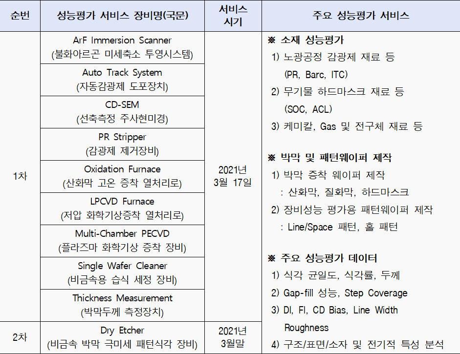
Building infrastructure capable of manufacturing 40nm patterned wafers
Support for future 20nm wafer manufacturing and component testing
Materials and components for semiconductor production are key items that raised awareness about the need for self-sufficiency in materials, components, and equipment (SME) technology in Korea following Japan's export restrictions in July 2019. Even before Japan's export restrictions, domestic semiconductor SME companies faced significant challenges due to the lack of 12-inch test beds comparable to the production environments of large corporations.
On the 17th, the Ministry of Science and ICT officially launched the service of the 12-inch semiconductor test bed built at the Nano Comprehensive Technology Institute (NCTI).
The material uniformity, defect, and other quality assessments required by semiconductor giants like Samsung Electronics and SK Hynix on 12-inch wafers were impossible in Korea. Consequently, most small and medium-sized enterprises (SMEs) were forced to either spend significant time and money on overseas test beds or settle for basic assessments using Jonggiwon's 8-inch equipment.
To address these issues, the Ministry of Science and ICT designated Jonggiwon as the operator of the 12-inch semiconductor small and medium-sized equipment test bed in August 2019, and invested a total of 45 billion won in national funds to build a clean room and 10 pieces of core equipment, and to promote equipment stabilization work, thereby launching official service. Semiconductor small and medium-sized enterprises can utilize this service to receive support for material performance testing.
Lee Jo-won, the president of Jonggiwon, said, “The current 12-inch test bed is an infrastructure capable of manufacturing 40nm patterned wafers, and we plan to intensively support the development of core semiconductor materials and equipment, such as photoresists,” and “In the future, we plan to promote the construction of additional equipment and the development of process technology that can support the manufacturing of 20nm-level patterned wafers and component testing.”
Comments
Related news
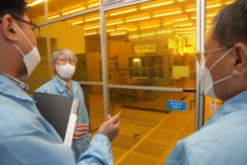
Will the 12-inch wafer-based micro-parts testbed yield results?
Minister Choi Ki-young of the Ministry of Science and ICT visited the on-site location of the 12-inch semiconductor materials, components, and equipment localization support testbed being established at the Nano Comprehensive Technology Institute, inspected the progress, and held a discussion meeting to activate the testbed. A total of 45 billion won will be invested in the Nano Comprehensive Technology Institute's construction of the 12-inch wafer-based semiconductor testbed from 2019 to 2022.
2020.08.13by 이수민 기자
A 5G network slicing testbed for SMEs is being built.
Small and medium-sized enterprises and venture companies are expected to find it easier to test and verify 5G content, convergence services, and infrastructure equipment that they develop in-house. The Korea Information Society Development Institute announced that it will, together with the Ministry of Science and ICT, establish a network slicing-based 5G testbed that supports small and medium-sized enterprises and venture companies in developing and testing 5G-based infrastructure equipment, terminals, devices, and convergence services.
2020.09.17by 이수민 기자
The Ministry of Trade, Industry and Energy will invest 5 trillion won to boost data and small business R&D.
The Ministry of Trade, Industry and Energy announced the 2021 Integrated Implementation Plan for Industrial Technology Innovation Projects, which contains a plan to support industrial technology R&D with a scale of 4.9518 trillion won. This represents an 18.7% increase compared to 2020 (4.1718 trillion won). In 2021, the Ministry of Trade, Industry and Energy will continuously expand investment in △materials, components, and equipment (MCE) sectors and △three major emerging industries for innovative growth (Big 3), strengthen investment in △the Korean version of the New Deal including the Green New Deal and Digital New Deal, and △the realization of carbon neutrality (net-zero) by 2030.
2020.12.30by 이수민 기자

Intel Unveils Next-Generation 'Core Ultra Series 3' and vPro Platform for Enterprise PCs
Intel has officially unveiled the "Intel Core Ultra Series 3" for next-generation enterprise PCs and the latest vPro platform, addressing a wide range of demands from enterprise notebooks to high-performance workstations.
2026.03.26by 배종인 기자

ROHM Launches ESD Protection Diode Compatible with High-Speed Interfaces of 10Gbps or Higher
Semiconductor specialist ROHM has developed the 'RESDxVx series' of ESD (electrostatic discharge) protection diodes capable of responding to next-generation high-speed data communication environments exceeding 10Gbps, simultaneously enhancing both signal quality maintenance required in high-speed interfaces and IC protection performance.
2026.03.26by 배종인 기자











