



To improve the accuracy of distance measurement and object detection of ToF systems
 Published2021.04.21 16:24
Can measure distances from less than 10cm to less than 15m
Need for assistance in solution to prevent distortion of measurement results
Distance measurement and object detection play a vital role in a variety of applications, including factory automation, robotics, and logistics. Safety-related applications in particular may require technology to detect and respond to objects or people at a certain distance. For example, a robot arm may need to stop immediately when a worker enters a danger zone.
Time of Flight (ToF) technology is increasingly being used for these purposes. ToF technology uses a modulated light source, such as a laser, to emit light, which then bounces off one or more objects and is captured by a sensor or camera.
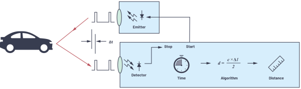
Knowing the time difference, ∆t, between when the light is emitted and when the reflected light is received, we can find the distance. This time delay is twice the distance between the camera and the object (round trip). Therefore, the distance can be calculated using the formula d = (c × ∆t) / 2, where c is the speed of light. The ToF camera outputs 2D data along with the required depth information.
ToF captures the entire image at once, scanning line by line, and does not require relative movement between the sensor and the target object. ToF is classified as Light Detection And Ranging (LiDAR), but is strictly a "flash" LiDAR-based technique, not a "scanning" one.
There are basically two methods that can be used to measure the time of flight of an optical pulse using ToF: pulse operation based on CCD (Charge Coupled Device) technology, and CW (Continuous Wave) operation. Pulse mode measures the time elapsed between the time an optical pulse is emitted and received, while CW mode calculates the phase shift between the emitted modulated optical pulse and the received modulated optical pulse. Both methods have their own advantages and disadvantages.
Pulse mode emits light with high energy and short pulses, and is more robust to ambient light, making it more suitable for outdoor applications. On the other hand, CW mode is easier to implement, as the light source does not need to be extremely short, and the rising/falling edges are fast. However, it becomes difficult to implement when high-precision requirements require high-frequency modulation signals.
High chip resolution is possible depending on the existing pixel size, so it can recognize objects and movements as well as measure distances. The measurement distance can be from less than a few centimeters (<10cm) to less than a few meters (<15m). However, not all objects can be detected at the same level. The measurement results can vary depending on the condition, reflectivity, speed, etc. of the object. Measurement results can also be distorted by environmental factors such as fog or strong sunlight.
Analog Devices (ADI) offers comprehensive 3D ToF solutions to support rapid implementation of 3D ToF systems. These solutions integrate data processing, laser drivers, power management, and software/firmware into a single unit. Therefore, only an emitter to emit frequency-modulated optical signals and a detector to detect reflected signals are required as separate additional components. The figure below shows a block diagram of the solution.
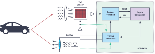
Such systems can be easily developed using an analog front end (AFE) with depth calculation capabilities. The ADI 'ADDI9036' is such a product, a comprehensive CCD ToF signal processor that integrates a laser diode driver, a 12-bit ADC, and a high-precision clock generator (for timing the CCD and laser). The ADDI9036 processes raw image data from a VGA CCD sensor to generate depth/pixel data.
ADI also works with design partners to provide integrated modules or development platforms. Users can develop their own specific algorithms using these evaluation systems and use these modules and platforms to reduce development time. This is useful for the development of industrial facilities and electrical equipment where pressure for rapid development is increasing.
This article is a summary of the article titled 'Time of Flight System for Distance Measurement and Object Detection' by Thomas Brand, FAE, Analog Devices (ADI).
References, " 3D Imaging with ADI Time of Flight Technology " ADI, 2020.
Comments
Related news
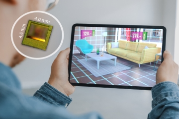
'3D Image Sensor' Capable of Implementing AR 10m Ahead to Be Released
Infineon Technologies and pmd technologies' 3D depth sensor based on ToF (Time of Flight) technology delivers innovative consumer convenience with superior performance that exceeds other solutions in the market. This 3D image sensor enables faster autofocus in low-light conditions or beautiful night mode portrait photography based on image segmentation, allowing for higher quality photos. Furthermore, it provides an unprecedented 10-meter long-range distance with minimal power consumption and enables the most immersive and smart AR experience implementation.
2020.10.30by 김동우 기자
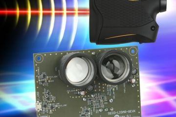
ON Semi Launches dToF LiDAR Platform Utilizing SiPM Technology
LiDAR applications are actively being utilized across all fields including the robotics industry and industrial proximity sensing, where millimeter-level accuracy is essential. On the 10th, ON Semiconductor unveiled a new direct time-of-flight (dToF) LiDAR solution based on SiPM (Silicon Photomultiplier) technology. The SiPM dToF LiDAR platform can detect objects within a distance range of 10 cm to 23 m. Additionally, it provides an out-of-the-box experience (OOBE) through a GUI that enables engineers to immediately begin technology evaluation. The platform design complies with IEC/EN 60825-1:2014 and 21 CFR 1040.10 and 1040.11 laser safety standards and has obtained FDA certification.
2020.11.10by 강정규 기자
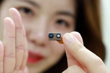
LG Innotek Develops ToF Module Dedicated to MS Azure Cloud
LG Innotek announced that it has signed an MOU with Microsoft for joint development and supply cooperation of a ToF module dedicated to Azure Cloud. The ToF module to be developed through the cooperation of both companies is intended to be mounted on wearable devices and serve as a data input device that interworks with Azure Cloud, with mass production targeted for the second half of this year.
2021.03.09by 이수민 기자

Intel Unveils Next-Generation 'Core Ultra Series 3' and vPro Platform for Enterprise PCs
Intel has officially unveiled the "Intel Core Ultra Series 3" for next-generation enterprise PCs and the latest vPro platform, addressing a wide range of demands from enterprise notebooks to high-performance workstations.
2026.03.26by 배종인 기자

ROHM Launches ESD Protection Diode Compatible with High-Speed Interfaces of 10Gbps or Higher
Semiconductor specialist ROHM has developed the 'RESDxVx series' of ESD (electrostatic discharge) protection diodes capable of responding to next-generation high-speed data communication environments exceeding 10Gbps, simultaneously enhancing both signal quality maintenance required in high-speed interfaces and IC protection performance.
2026.03.26by 배종인 기자











