


ETRI develops processes and materials that address challenges in micro LED production.
 Published2021.05.25 09:31
Significantly reduce equipment investment costs and process time by 1/10
Related products are expected to be commercialized within two years.
The Electronics and Telecommunications Research Institute (ETRI) announced on the 25th that it had solved the challenges of micro LED displays by independently developing new methods and materials. Micro LED displays are self-luminous displays that use 10-100㎛ (micrometer) LEDs as pixel light sources.
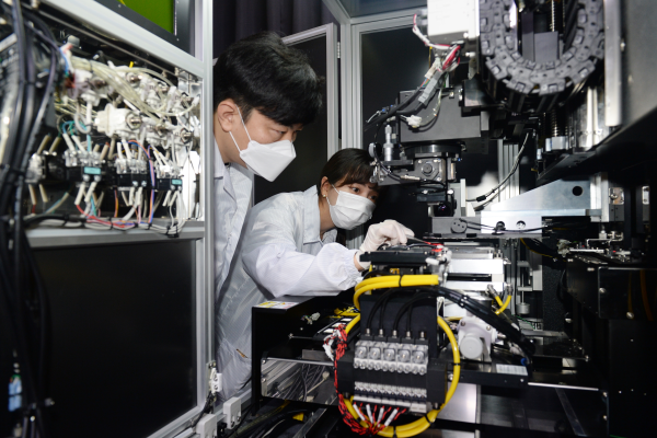
ETRI researchers have developed a micro LED transfer-bonding process.
Performance [Photo = ETRI]
Micro LED displays, which can produce more vivid colors and have higher luminous efficiency than LCD or OLED displays, are used in a variety of fields, including TVs and smartwatches. Separate control of RGB elements allows for precise display of screen brightness and color, and the use of inorganic materials ensures long-term use without the worry of burn-in.
According to market research firm Omdia, the Micro LED market is projected to grow at a compound annual growth rate of 65%, reaching $71 billion by 2027. In particular, Micro LED smartwatches are expected to exceed 10 million units, and Micro LED TVs are expected to exceed 3.3 million units. However, the high manufacturing difficulty has hindered the widespread adoption of Micro LED displays.
To create a micro LED display, micro LEDs must be created using a semiconductor process and then transferred to a display panel. For 8K TVs, the number of micro LEDs required reaches 100 million, and their size is so small that transplanting them takes a long time. The materials needed for display production are also imported, making them very expensive.
All methods announced so far have involved a "transfer" process for transferring the LEDs, followed by a "bonding" process for planting them. ETRI, however, has combined the transfer and planting processes into one using SITRAB film, a new material developed through its own research.
This process involves simultaneously transferring and bonding micro LEDs by firing a uniformly focused laser beam onto the SiteLab film for a few seconds. Even when the laser beam is applied uniformly over a wide area, only the desired area is selectively heated, allowing the micro LEDs to adhere. This eliminates the inconvenience of separate transfer and planting processes.
The development of a new material suitable for this method has paved the way for its use in displays, including micro LEDs and mini LEDs. The newly developed material allows for additional micro LEDs to be attached even after multiple laser exposures, making it significantly easier to repair defective pixels. This also overcomes the limitations of existing processes that previously prevented repairs.
Applying the technology developed by ETRI can reduce the investment costs for transfer equipment and bonding equipment that previously required large-scale investments, simplify the process, and lower the defect rate. When applied to actual industrial sites, it is expected that compared to existing methods, equipment investment costs and process time can be reduced to 1/10, and material costs, repair costs, and time can be reduced to less than 1/100.
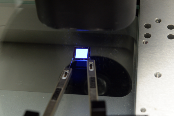
The micro LED display prototype unveiled by the research team targets the blue color within the RGB spectrum, featuring 1,225 micro LEDs embedded within an area of 100㎟. This represents 12 LEDs per 1㎟. ETRI estimates that if this technology is transferred to domestic display companies, related products could be commercialized within two years.
Comments
Related news
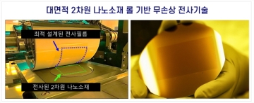
Korea Institute of Machinery and Materials (KIMM) is producing large, affordable transparent displays and semiconductors.
The Korea Institute of Machinery and Materials (KIMM, Director Park Sang-jin) under the Ministry of Science and ICT has developed "large-area 2D nanomaterial damage-free roll transfer technology" that enables the transfer of atomic layer-thick 2D nanomaterials at wafer scale without damage. This breakthrough improvement in the nanomaterial transfer process, which can be applied to various fields including transparent displays, transparent semiconductors, and displays for autonomous vehicles, is expected to accelerate technology commercialization.
2021.05.12by 배종인 기자

KAIST Develops Display-Driven OLED Electronic Textiles
Display-capable organic light-emitting diode (OLED) electronic fibers have been developed, and are expected to enable applications in fashion and functional clothing.
2021.05.13by 배종인 기자
Inorganic-based semiconductors to rise "also cheaper"
Adhesive health monitoring devices and foldable and rollable displays require flexible semiconductors. Most flexible semiconductors are organic-based, but a research team at UNIST's School of Advanced Materials Engineering has developed an inorganic-based flexible semiconductor. Since it can withstand high-temperature, high-pressure processes and exhibits good durability, it is expected to be applicable to the development of various flexible devices.
2021.05.17by 이수민 기자

Intel Unveils Next-Generation 'Core Ultra Series 3' and vPro Platform for Enterprise PCs
Intel has officially unveiled the "Intel Core Ultra Series 3" for next-generation enterprise PCs and the latest vPro platform, addressing a wide range of demands from enterprise notebooks to high-performance workstations.
2026.03.26by 배종인 기자

ROHM Launches ESD Protection Diode Compatible with High-Speed Interfaces of 10Gbps or Higher
Semiconductor specialist ROHM has developed the 'RESDxVx series' of ESD (electrostatic discharge) protection diodes capable of responding to next-generation high-speed data communication environments exceeding 10Gbps, simultaneously enhancing both signal quality maintenance required in high-speed interfaces and IC protection performance.
2026.03.26by 배종인 기자











