



STMicroelectronics Announces First Production of 200mm SiC Wafers, Procuring 40% of the Production In-House
 Published2021.08.10 08:32
First 8-inch SiC bulk wafers produced in Sweden
Plans to produce 40% of our consumption in-house by 2024
STMicroelectronics announced on the 9th that it has produced prototype 200mm (8-inch) silicon carbide (SiC) bulk wafers at its facility in Norrköping, Sweden, which have reduced defect rates by minimizing crystal dislocation defects.
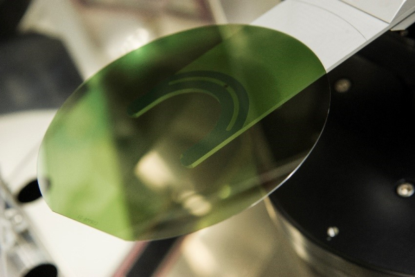
The low wafer defect rate was achieved based on the expertise of SiC ingot growth technology developed by STMicroelectronics Silicon Carbide, formerly Norstel, which ST acquired in 2019.
The transition to 200mm SiC wafers requires the development of a comprehensive support ecosystem, including equipment suppliers, to address quality issues. ST is developing its own 200mm SiC manufacturing equipment and process technology in collaboration with multiple technology partners across the entire supply chain.
ST is currently producing STPOWER SiC products in volume on two 150mm wafer lines at its Catania, Italy, and Ang Mo Kio, Singapore, fabs, with assembly and testing taking place at its back-end facility in Shenzhen, China. ST plans to build a new SiC wafer facility and procure more than 40% of its SiC wafers internally by 2024.
SiC is a compound semiconductor material that offers higher performance and efficiency than silicon (Si) in power applications. ST's 25 years of R&D have resulted in over 70 patents. A 200mm wafer can produce integrated circuits with nearly twice the usable area of a 150mm wafer, providing 1.8 to 1.9 times more working chips.
Comments
Related news
The Ministry of Trade, Industry and Energy announced that the power semiconductor commercialization project achieved 39 billion won in results.
The Ministry of Trade, Industry and Energy conducted a review on the 21st of the commercialization project outcomes for power semiconductors aimed at creating new industries. The project has been carried out from 2017 through 2023 to establish a domestic industrial foundation for power semiconductors based on compound materials such as Si, SiC, and GaN. During this review, it was confirmed that commercialization results worth approximately 39 billion won were generated from 2019 through May of this year through product development by participating companies.
2021.07.21by 이수민 기자
Microchip Launches 1700V SiC Solution to Replace Si IGBTs
Today's electric charging systems that enhance propulsion in commercial vehicles, auxiliary power systems, solar inverters, semiconductor transformers, and other transportation and industrial applications all rely on high-voltage switching power devices. In response, Microchip has expanded its SiC portfolio by launching 1700V SiC MOSFET dies, discretes, and power modules.
2021.07.28by 이수민 기자

SK Siltron Continues Investment in SiC Wafers
SK Siltron (CEO Jang Yong-ho) is drawing attention as it continues to invest in SiC wafer production, a SiC semiconductor material expected to see increased demand in electric vehicles and other applications, through debt guarantees, facility expansion investments, and other ongoing capital commitments.
2021.08.04by 배종인 기자

Intel Unveils Next-Generation 'Core Ultra Series 3' and vPro Platform for Enterprise PCs
Intel has officially unveiled the "Intel Core Ultra Series 3" for next-generation enterprise PCs and the latest vPro platform, addressing a wide range of demands from enterprise notebooks to high-performance workstations.
2026.03.26by 배종인 기자

ROHM Launches ESD Protection Diode Compatible with High-Speed Interfaces of 10Gbps or Higher
Semiconductor specialist ROHM has developed the 'RESDxVx series' of ESD (electrostatic discharge) protection diodes capable of responding to next-generation high-speed data communication environments exceeding 10Gbps, simultaneously enhancing both signal quality maintenance required in high-speed interfaces and IC protection performance.
2026.03.26by 배종인 기자











