



"Advanced packaging is necessary for the semiconductor ecosystem to mature"
 Published2022.08.26 12:00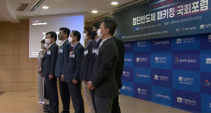
▲첨단반도체 패키징 국회포럼 (사진-서울테크노파크)
전문가들, "설계·제조·패키지 3축 시너지 통해 생태계 구축 가능"

반도체 미세공정이 한계에 다다르고 있다는 우려가 커지는 가운데 전세계 1,000억달러 시장에 육박하는 반도체 패키징 분야를 차세대 전략 산업으로 성장시켜야 한다는 논의의 장이 마련됐다.
‘첨단반도체 패키징 국회포럼’이 25일 여의도 의원회관 제2소회의실에서 서울과학기술대학교와 서울테크노파크 주관으로 개최했다. 이날 포럼에는 이강욱 SK하이닉스 부사장, 김동현 하나마이크론 부사장 등이 참여해 패키징 기술 강연을 진행했다.
이날 포럼은 반도체 설계·제조·후공정 3축이 동시에 진흥될 때 반도체 생태계가 시너지효과를 낼 수 있다며 국내 패키징 산업의 발전방안을 모색했다.
변재일 더불어민주당 국회의원은 “중국과 대만 중심으로 패키징 산업이 발전했으며 국내는 상대적으로 뒤쳐져 있다”며 “현재 정부의 추진 예타사업을 보면 패키징 분야에 우려감을 못 느끼고 있다고 본다”고 우려했다. 그는 “관계자들이 비싼 국내 패키징에 의뢰하느니 대만에 의뢰하는 게 더 저렴하다며 도외시하는 의견들을 들었다”며 패키징에 대한 중요성이 경시되고 있다고 토로했다. 후공정 문제에 대해 기술적 문제뿐 아니라 정책 비전의 제시가 필요하다고 피력했다.
■ 반도체 산업 과거는 덧셈의 공식, 지금은 곱셈
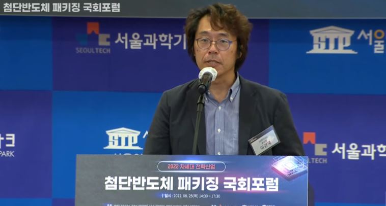
▲이강욱 SK하이닉스 부사장 (사진-서울테크노파크)
“과거는 덧셈의 공식이 적용돼 패키징 공정이 약해도 디자인과 팹(전공정)을 통해 제품 경쟁력을 가질 수 있었지만 현재는 곱셉의 공식으로 바뀌며 설계, 팹, 패키징 어느 하나도 도외시할 수 없으며 하나라도 0이 된다면 비즈니스가 성립되기 어렵다”
이강욱 SK하이닉스 부사장은 이날 포럼에서 연사로 나와 ‘반도체 산업 혁신을 위한 반도체 패키징 기술의 역할’을 강연했다. 그는 반도체 패키징이 최근 제품의 가치를 높이며 새로운 사업의 영역으로 급부상하고 있다고 언급했다.
이강욱 부사장은 “현직에 있으면서 패키징의 중요성을 피부로 느끼며, 글로벌 기업들이 관련 헤게모니를 잡기 위한 경쟁이 치열하다는 것을 직접 보고 있다”며 “메모리 반도체 강국에서 종합 반도체 강국으로 가기 위해서는 패키징 기술이 지렛대 역할을 할 것”이라고 분석했다.
최근 업계 동향은 이종집적화(칩렛) 기반의 솔루션 플랫폼 확보 경쟁이 가속화하고 있다. TSMC가 현재 이와 관련한 후공정 부문에서 기술력을 앞세워 시장을 독점하다시피 하고 있으며, 이는 솔루션 중심의 파운드리 비즈니스를 영위하는 모델을 선택해 고객사들로부터 선호 받고 있다.
인텔은 팹 중심으로 매출 증대를 위해선 투자 또한 비례해 증가하게 된다. 또한 인텔 및 삼성이 IDM 기업이기에 기술 노하우 등의 유출을 꺼려하는 고객사들로부터 선호되기 어려운 점도 한몫한다.
이 부사장은 “대만은 팹리스-파운드리-메모리-EMS-OSAT 간의 밸류체인이 공고하다”고 평가하며 한국이 종합반도체로 가기 위해선 첨단 패키징 기술 기반 반도체 산업 혁신이 필요하다고 제언했다. 이를 위한 △인재육성 △통합 R&D △후공정 분야 소부장 및 파운드리-IDM-OSAT 간 생태계 강화를 함께 제시했다.
과거 대비 현재 패키징 기술 난도 오르면서 설계-팹-패키징 기술이 융복합되는 트렌드 보이고 있다. 이 부사장은 “소재 및 장비의 고가화로 인해 중소 소부장이나 OSAT쪽이 첨단 패키징 영역을 확보하긴 어려울 것”이라며 “파운드리와 IDM 기업들이 이끌어가게 될 것”으로 내다봤다.
국내는 메모리 반도체 중심의 성장으로 OSAT 및 후공정 생태계 경쟁력이 취약한 상태이다. 전문 인력 교육·양성 체계가 미흡하다는 이 부사장은 “후공정 분야 산학연 통합 연구개발을 체계적으로 주도할 컨트롤 타워가 필요하다”고 덧붙였다.
■ 응용·융합 분야에서의 패키징 가치↑
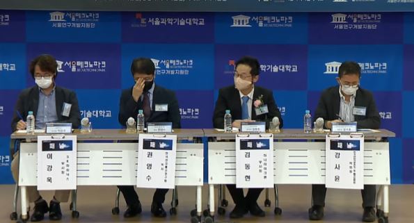
▲왼쪽부터 SK하이닉스 이강욱 부사장, 한국전자통신연구원 권영수 박사, 하나마이크론 김동현 부사장, 한국마이크로전자 및 패키징학회 강사윤 학회장이 패널토의를 진행하는 모습 (사진-서울테크노파크)
첨단 패키징은 자율주행, 하이퍼스케일 AI, 고성능 컴퓨팅(HPC) 등 응용·융합 분야로의 확대가 진행되고 있으며, 관련 기술력이 해당 분야의 성패를 좌우할 만큼 중요성이 커지고 있다.
한국전자통신연구원 권영수 박사는 “하이퍼스케일 AI가 보편화하기 위해선 반도체 혁신이 필수적”이라며 AI분야 거대 인공신경망은 나날이 발전해 학습된 데이터의 개수인 파라미터가 100조개에 이르렀다고 강조했다. 권 박사는 이러한 하이퍼스케일 AI를 담을 반도체가 없기에 국내에서 인공지능 파라미터의 구축이 어렵다고 토로했다.
레티클 사이즈 등 물리적 한계와 과다한 개발비용 등으로 인해 하이퍼스케일 AI 구현을 위해 필요한 해법은 인터포저와 같은 첨단 패키지가 대두되고 있으며 이러한 패키지를 통해 NPU, HBM, S램 등 많은 다이를 하나의 칩에 집적해 단일 프로세서로 연결시켜 동작하는 반도체가 등장한 배경이 되는 것이다. 권 박사는 이것이 성능 및 전력 등의 문제를 해결할 수 있다고 설명했다.
자율주행 분야에서도 인공지능 알고리즘 중요하며 이를 위한 핵심은 하드웨어 기술이다. 하나마이크론 김동현 부사장은 테슬라 Dojo D1칩을 언급하며 자율주행용으로 쓰이는 AI반도체가 하이퍼스케일 구현을 위한 칩을 제작하기 위해선 첨단 패키징 기술이 필수적이라고 강조했다.
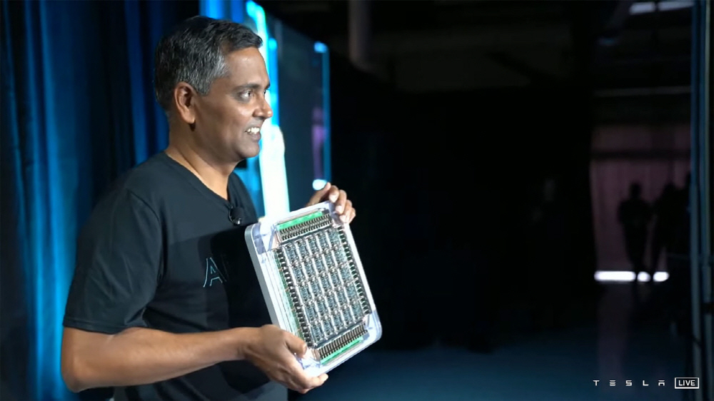
▲ D1칩 25개가 집적된 멀티칩 모듈 (사진-테슬라 라이브)
반면 대기업이나 서버시장은 가격이 비싸도 AI반도체를 쓸 수 있지만 보편화되기 위해선 저비용이어야 한다. 실리콘 인터포저가 적용된 칩렛은 1000불 가까이 더 비싸지는 비용적 어려움을 맞닥뜨리게 된다고 김 부사장은 지적했다.
통신용 반도체 부문에서는 패키징 기술이 가장 발달한 부분이다. 고주파 영역 사용으로 인해 실리콘으론 고출력을 감당할 수 없어 이종집적화가 빠르게 일어난 부문이다. 차세대 통신 반도체 기술은 밀리미터파와 테라헤르츠 안테나를 위한 패키징 기술이 필요하다고 밝혔다.
한국마이크로전자 및 패키징학회 강사윤 학회장은 패키징의 시대가 도래한 이유를 전공정의 한계와 다양한 IT의 출현으로 꼽았다. 웨어러블, AR·VR 등이 등장하며, 다양한 IT기기의 가짓수를 기존 IDM이 커버할 수 없었기 때문이다.
강 학회장은 “향후 AI로 반도체 전환기가 일어날 것이며 2030년까지 반도체 매출이 1조2,000달러에 이를 것”이라고 전망했다. 데이터 중심의 AI가 핵심이 될 것으로 내다봤다.

Comments
Related news
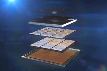
As demand for high-performance semiconductors grows, the importance of post-process packaging grows.
Packaging, a representative post-process in semiconductor manufacturing, is the process of encapsulating devices fabricated in the front-end process to produce finished products. The industry is taking note of it as a key technology for high integration and multi-functional implementation of devices. Advanced packaging technology that integrates multiple devices into one is replacing traditional packaging technology, which aims at electrical connection and protection of semiconductor devices.
2021.09.13by 이수민 기자
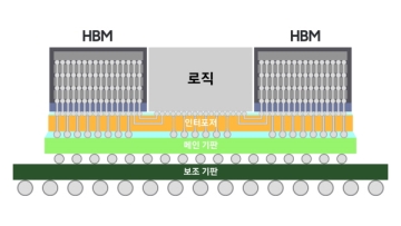
Samsung Electronics Leads the Industry with Next-Generation Semiconductor Packaging Technology
Samsung Electronics is expanding its supply of high-performance semiconductors through next-generation semiconductor packaging technology.
2021.11.11by 배종인 기자
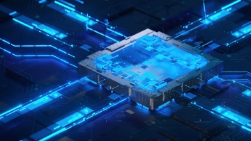
Intel Unveils Latest Architecture and Packaging Innovations at Hot Chips 34
The semiconductor industry is entering a golden age that requires a paradigm shift from the traditional foundry model to the systems foundry model. Intel's systems foundry model goes beyond conventional wafer manufacturing support to offer Systems-in-Package that integrates △advanced packaging △open chiplet ecosystems △software components, focusing on meeting the needs of users demanding powerful computing capabilities and immersive digital experiences.
2022.08.25by 명세환 기자

Intel Unveils Next-Generation 'Core Ultra Series 3' and vPro Platform for Enterprise PCs
Intel has officially unveiled the "Intel Core Ultra Series 3" for next-generation enterprise PCs and the latest vPro platform, addressing a wide range of demands from enterprise notebooks to high-performance workstations.
2026.03.26by 배종인 기자

ROHM Launches ESD Protection Diode Compatible with High-Speed Interfaces of 10Gbps or Higher
Semiconductor specialist ROHM has developed the 'RESDxVx series' of ESD (electrostatic discharge) protection diodes capable of responding to next-generation high-speed data communication environments exceeding 10Gbps, simultaneously enhancing both signal quality maintenance required in high-speed interfaces and IC protection performance.
2026.03.26by 배종인 기자











