


[Semiconductor Show 2022] CEO Kwak No-jeong: "Development of new materials to overcome memory limitations is essential."
 Published2022.10.06 10:43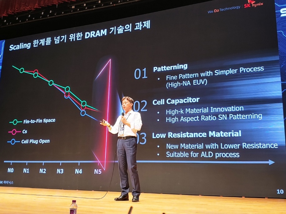
▲SK Hynix CEO Kwak No-jeong delivers a keynote speech at Semiconductor World Congress 2022.
3D stacked DRAM and TLC NAND are expected to evolve into QLC and PLC.
Development of materials such as high-K, contact resistance, and low-resistance WL is essential.
Innovation in high-k materials is essential. New materials must be developed to address the resistance issues associated with shrinking contact sizes.
These are the words of SK Hynix CEO Kwak No-jeong, speaking on the topic of “Beyond the Limits of Memory Technology” at the 2022 Semiconductor Expo keynote event hosted by the Semiconductor Industry Association on the 5th.
CEO Kwak predicted that data usage has increased sharply since the proliferation of smartphones, and that cars will begin generating 40 terabytes (TB) of data per hour as they become increasingly equipped with autonomous driving features, communications, and electronic components. Accordingly, he predicted that the connected mobility market, encompassing advertising, insurance, and finance, will grow to over 10 trillion won annually by 2030.
Semiconductor technology is what enables processing this exploding data and driving market growth in related industries. The need for innovation in memory technology has long demanded a similar direction. The three key characteristics are △large capacity △high speed △low power.
Experts agree that while DRAM has begun mass production at the 10nm level through continuous scaling down, the limits of process miniaturization have been reached. CEO Kwak also predicted significant resistance to scaling down at the 10nm level due to factors such as reduced fin spacing and increased contact resistance due to smaller contact sizes, stating, "High NA EUV will absolutely be necessary for patterning."
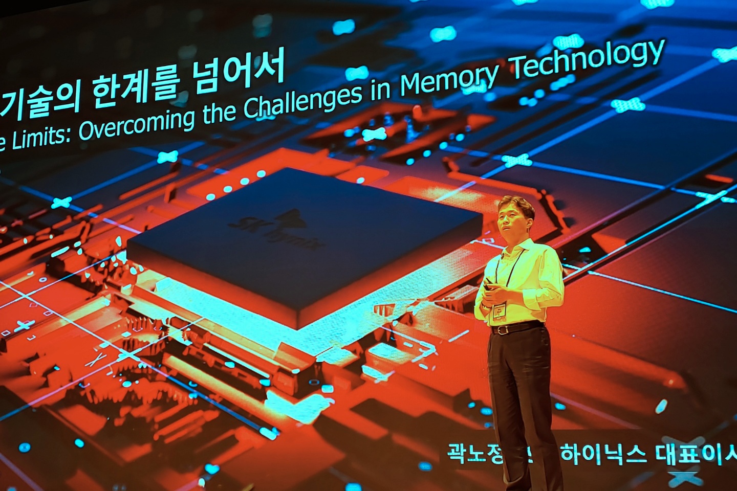
▲ Kwak No-jeong, CEO of SK Hynix
He emphasized that innovation in "high-k materials" is necessary, particularly considering the capacitance issue of cell capacitors. He also added that new materials must be developed to address resistance issues resulting from shrinking contact sizes.
SK Hynix is researching and developing a new platform as a new scaling alternative. CEO Kwak stated, "We are considering applying 3D stacking technology to DRAM, similar to NAND flash." It is already known that Samsung Electronics and Micron of the United States are researching and developing 3D DRAM for next-generation products.
NAND flash technology has recently succeeded in developing 238-layer NAND flash through stacking technology, but CEO Kwak expressed concern, saying, “I am concerned about whether it will be possible to go beyond 400 layers.”
While increasing the number of NAND layers is necessary, the absolute height needs to be reduced. This necessitates the development of technologies to reduce oxide film thickness. Furthermore, as the number of layers increases, future challenges remain, such as how many NAND flashes after single-stack stacking (double-stack, triple-stack, etc.) should be connected to increase the number of layers, and how to reduce the associated costs.
CEO Kwak predicted that in order to improve the number of bits per unit area of NAND, “Currently, mass production of TLC (Triple Level Cell) is the main focus, but in the future, the trend will change to QLC (Quad Level Cell) and even PLC (Penta Level Cell).”
NAND flash is expanding its storage capacity through lateral scaling, which will require improved WL filling and low-resistance WL materials. CEO Kwak added, "Wafer bonding will be applied in the future."
Meanwhile, Semiconductor Expo 2022, featuring domestic and international semiconductor companies such as Samsung Electronics and SK Hynix, opened on the 5th and is currently underway at COEX in Samseong-dong, Seoul, for three days. This event, which showcases solutions for strengthening the semiconductor ecosystem and various semiconductor technologies, materials, components, and equipment, boasts 235 companies and 800 booths, making it the largest event ever and attracting significant attention.
(Reporter Kwon Shin-hyeok)

Comments
Related news
SK Hynix to produce 100% domestically produced neon by 2024
SK Hynix will achieve 100% localization of 'neon (Ne) gas,' used in semiconductor photolithography processes, in 2024, and will make full-scale efforts to strengthen the semiconductor raw material supply chain.
2022.10.05by 배종인 기자
[Semiconductor Show 2022] Strengthening the Semiconductor Ecosystem… 235 Companies and 800 Booths Participating
As the environment surrounding the semiconductor industry undergoes significant change, the responsiveness of related companies has become a critical point in time. At the semiconductor exhibition, which brings together domestic and international semiconductor companies on a record-breaking scale, visitors continue to flock in.
2022.10.05by 명세환 기자
.jpg)
[Semiconductor Expo 2022] Korea University BASIC Lab Wins Presidential Award at Design Expo
The foundation for strengthening the system semiconductor ecosystem relies significantly on talent development. In response to this need, a competition was held to foster creativity among talent in the semiconductor design field and enhance design capabilities.
2022.10.06by 명세환 기자

Intel Unveils Next-Generation 'Core Ultra Series 3' and vPro Platform for Enterprise PCs
Intel has officially unveiled the "Intel Core Ultra Series 3" for next-generation enterprise PCs and the latest vPro platform, addressing a wide range of demands from enterprise notebooks to high-performance workstations.
2026.03.26by 배종인 기자

ROHM Launches ESD Protection Diode Compatible with High-Speed Interfaces of 10Gbps or Higher
Semiconductor specialist ROHM has developed the 'RESDxVx series' of ESD (electrostatic discharge) protection diodes capable of responding to next-generation high-speed data communication environments exceeding 10Gbps, simultaneously enhancing both signal quality maintenance required in high-speed interfaces and IC protection performance.
2026.03.26by 배종인 기자











