


ADI: "'ADALM2000' LC Oscillator Resonance Characteristics Visually Confirmed"
 Published2026.03.09 14:42
단순히 ‘발진한다’ 넘어 왜 제한되는지·어떻게 개선되는지 검증
이 글에서는 아나로그디바이스의 ADALM2000 교육용 키트를 활용하여 펠츠 오실레이터 구성의 특성을 살펴보는 실습 과정을 소개한다.
■ 두 개의 트랜지스터를 사용하는 펠츠(Peltz) 오실레이터
클랩(Clapp), 콜피츠(C·lpitts), 하틀리(Hartley) 오실레이터가 한 개의 트랜지스터를 사용하는 것과 달리, 펠츠(Peltz) 오실레이터는 두 개의 트랜지스터를 사용한다.
그림 1을 보면 트랜지스터 Q1은 공통 베이스 증폭기 단으로 구성되어 있다.
L1과 C1으로 이루어진 공진 탱크는 컬렉터 부하를 제공한다. 컬렉터에서의 출력은 이미터 팔로어(공통 컬렉터) 단으로 구성된 트랜지스터 Q2의 베이스로 전달된다.
발진에 필요한 양(+)의 피드백은 이미터 팔로어의 출력(Q2의 이미터)을 공통 베이스 단의 입력인 Q1의 이미터로 다시 연결함으로써 형성된다.
공통 베이스 증폭기 단의 전압 이득은 LC 탱크의 병렬 공진 주파수에서 최대가 되는데, 이때 임피던스는 무한대에 가까워진다.
이미터 팔로어의 이득은 항상 1보다 약간 작다. 공진 시 루프 전체의 결합 이득은 1보다 훨씬 커져 발진을 지속할 수 있다.
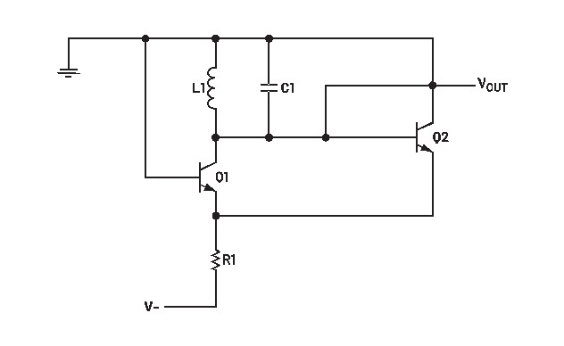
▲그림 1. 기본적인 펠츠 오실레이터 구성
LC 탱크의 공진 주파수는 공식 1로 구할 수 있다.

이 오실레이터 구성에서는 LC 탱크 양단의 피크-투-피크 스윙이 제한된다.
Q2의 베이스 전압이 접지보다 더 양(+)으로 스윙하면 Q2의 컬렉터-베이스 접합이 순방향으로 바이어스되어, 최대 양의 스윙이 약 한 개의 순방향 다이오드 전압 강하 정도로 제한된다.
최대 음(-)의 스윙에서도 마찬가지로, Q1의 컬렉터 전압이 충분히 음으로 스윙하면 Q1의 컬렉터-베이스 접합이 순방향 바이어스된다.
BJT 트랜지스터의 컬렉터-베이스 접합이 순방향 바이어스되면 베이스 전류가 급격히 증가한다.
이 증가된 베이스 전류를 이용하면 LC 탱크 양단에서 관측되는 피크-투-피크 스윙을 증가시킬 수 있다.
그림 2와 같이 Q1과 Q2의 베이스에 각각 직렬로 저항을 삽입하면, LC 탱크 전압의 극한 값에서 저항을 통해 흐르는 추가 전류로 인해 Q1과 Q2의 베이스 전압이 더 낮아진다.
.jpg)
▲그림 2. 증가한 출력 스윙

■ 실험 전 시뮬레이션
그림 1 및 그림 2와 같이 펠츠 오실레이터의 시뮬레이션 회로도를 작성한다.
트랜지스터 Q1과 Q2에서 각각의 컬렉터 전류가 200μA보다 크도록 바이어스 저항 R1의 값을 계산한다.
회로는 -5V 전원으로 구동된다고 가정한다.
공진 주파수가 최소 1MHz 이상이 되도록 C1과 L1의 값을 계산한 후, 과도 응답 시뮬레이션을 수행한다.
LC 탱크 양단의 피크-투-피크 출력 스윙은 순방향 다이오드 전압 강하(약 ±0.6 V)보다 작게 제한되어야 한다.
출력 스윙이 최소 ±1.25V 이상으로 증가하도록 R2 = R3의 값을 계산하고 시뮬레이션을 수행한다. 이 결과를 저장해 실제 회로에서 측정한 값과 비교하고, 실험 보고서에 포함시킨다.
■ 실험 자재 목록
· ADALM2000 능동 학습 모듈
· 솔더리스 브레드보드
· 점퍼 와이어
· 소신호 NPN 트랜지스터 2개(2N3904)
· 10kΩ 저항 1개
· 4.7kΩ 저항 2개
· 100μH 인덕터 1개
· 100pF 커패시터 1개
■ 지침
솔더리스 브레드보드를 사용해 그림 3에 제시된 펠츠 오실레이터 회로를 구성한다. 사각형 표시는 ADALM2000 모듈의 오실로스코프 채널과 전원 공급 장치를 연결할 위치를 나타낸다. 전원 공급 장치를 켜기 전에 반드시 배선을 한 번 더 확인한다.
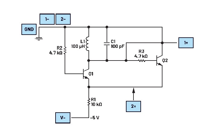
▲그림 3. 펠츠 오실레이터 회로
■ 하드웨어 설정
두 개의 오실로스코프 입력을 모두 200mV/div로 설정하고, 시간 기준은 1μs/div로 설정한다. 채널 1의 상승 엣지 상에 트리거를 설정한다. 브레드보드 회로는 그림 4를 참고하면 된다.
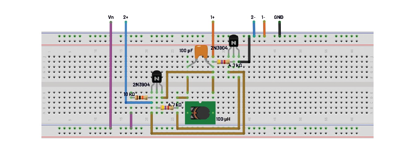
▲그림 4. 펠츠 오실레이터 회로의 브레드보드 연결
■ 절차
-5V 전원 공급 장치를 켠 후, 오실로스코프 채널 1에서 LC 탱크 양단의 출력 파형을 관찰한다. 이 파형은 오실로스코프 채널 2를 사용하여 Q1과 Q2의 이미터에서도 확인할 수 있다.
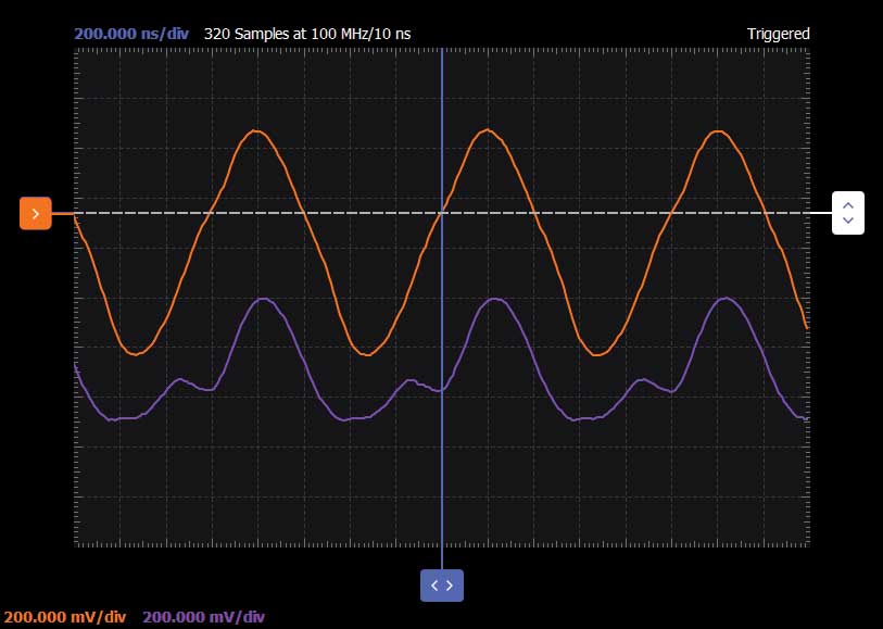
▲그림 5. 펠츠 오실레이터 회로 파형
■ 질문
1. 펠츠 오실레이터의 주요 기능은 무엇인가?
2. 펠츠 오실레이터는 어떤 오실레이터의 변형인가?
3. 펠츠 오실레이터를 콜피츠 및 클랩 오실레이터와 구별 짓는 구성 요소는 무엇인가?
4. 콜피츠나 클랩과 같은 다른 LC 오실레이터보다 펠츠 오실레이터가 선호되는 경우는 언제인가?
위 질문에 대한 답변과 추가적인 설명은 아나로그디바이스 StudentZ·ne 블로그 https://ez.anal·g.c·m/studentz·ne/에서 확인할 수 있다.
※ 저자 소개
안토니우 미클라우스(Antoniu Miclaus)는 아나로그디바이스(Analog Devices)에서 소프트웨어 엔지니어로, 리눅스 및 비OS(non-OS) 드라이버용 임베디드 소프트웨어 개발, ADI 학술 프로그램, 품질 보증(QA) 자동화, 프로세스 관리 등을 담당하고 있다. 그는 2017년 2월 루마니아 클루지-나포카(Cluj-Napoca)에 위치한 ADI에 입사했다. 그는 바베시-보요이 대학교(Babes-Bolyai University)에서 소프트웨어 공학 석사(M.Sc.), 클루지-나포카 공과대학교(Technical University of Cluj-Napoca)에서 전자 및 통신공학 학사(B.Eng.) 학위를 받았다.
Comments
Related news
[Technical Contribution] ADI: "Multiphase Flyback Converter Delivers Over 60W of Power"
Frederik Dostal, a power management expert at Analog Devices, Inc., discusses the design of flyback converters for high-power applications.
2025.10.13by 명세환 기자

ADI Innovates AI Embedded Development and Upgrades Open-Source Development Platform
Global semiconductor company Analog Devices, Inc. (ADI) has officially announced 'CodeFusion Studio™ 2.0,' a major upgrade to its open-source embedded development platform. This update focuses on simplifying and accelerating AI-based embedded systems development while providing a developer-centric integrated toolchain.
2025.11.04by 명세환 기자
ADI, “Simple and Efficient Voltage Inverting Possible Without 'LTC7899' Transformer”
We spoke with Frederik Dostal, power management expert at Analog Devices, Inc., about voltage conversion ICs in inverting topology.
2025.11.06by 명세환 기자
.jpg)
ADI, “Overvoltage Safety Protection with ‘LT4363’ MOSFET SOA Precision Management”
We spoke with Frederik Dostal, a power management expert at Analog Devices, Inc., about how to easily offset overvoltage using protection circuits.
2025.12.05by 명세환 기자
ADI Accelerates Smart Factory Network Integration with Industrial Ethernet TSN Switch ICs
Analog Devices, Inc. (ADI) announced that its industrial Ethernet TSN (Time-Sensitive Networking) switch ICs, the ADIN6310 and ADIN3310, have obtained CC-Link IE TSN recommended network wiring component testing (Class A·B) certification from the CC-Link Partner Association (CLPA).
2025.12.23by 명세환 기자











