


Applied Materials and SK Hynix Partner to Develop Next-Generation AI Memory
 Published2026.03.11 08:02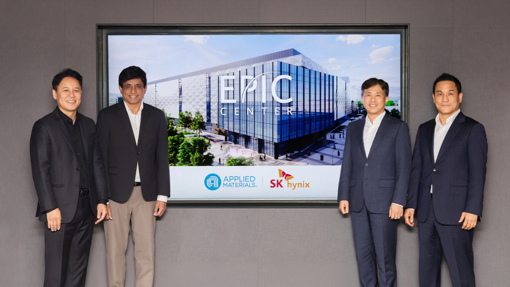
▲(From left) Park Kwang-sun, CEO of Applied Materials Korea; Prabhu Raja, President of Applied Materials Semiconductor Products Group; Kwak No-jung, CEO and President of SK Hynix; and Kang Yu-jong, Vice President of SK Hynix, pose for a commemorative photo after signing the MOU.
As competition intensifies to develop high-performance memory, a key component in the AI era, Applied Materials and SK Hynix have joined hands to jointly develop next-generation AI memory.
Applied Materials announced on the 11th that it has formed a long-term partnership with SK Hynix to jointly research and develop next-generation DRAM and HBM technologies.
The two companies will strengthen their collaboration centered around Applied's EPIC (Equipment and Process Innovation and Commercialization) Center currently under construction in Silicon Valley, and jointly pursue an innovation roadmap to respond to the expansion of AI infrastructure.
As the computational load of AI systems has recently exploded, memory speed and power efficiency have emerged as key challenges for the semiconductor industry.
SK Hynix CEO Kwak No-jeong emphasized, “The biggest obstacle to improving AI performance is the speed gap between processors and memory,” and “To solve this, faster and more efficient memory technology is essential.”
This collaboration is a strategic choice to address these industrial needs, and both companies We are driving innovation across all areas of memory, from new material exploration to process integration and 3D packaging.
Applied Materials is dramatically revolutionizing its semiconductor equipment and process R&D methods through its EPIC Center, scheduled to open this year.
The $5 billion center is considered the largest semiconductor equipment research investment in the United States.
SK Hynix engineers will reside at the EPIC Center and collaborate directly with Applied Technologies' technical staff. This will accelerate the validation of new technologies and shorten the time to mass production.
“Our two companies have a long history of working together on materials engineering-based memory innovation,” said Gary Dickerson, CEO of Applied Materials. “Our collaboration at the EPIC Center will be a significant turning point in accelerating the commercialization of next-generation DRAM and HBM.”
Initial joint research will focus on new material development, process integration technology, and HBM-level advanced packaging.
SK Hynix CTO Cha Seon-yong explained, “In the era of AI memory, existing wafer fab equipment development methods have limitations,” and “A new approach is needed across all areas, including new materials, thermal management, and packaging.”
SK Hynix also plans to leverage Applied Materials' advanced packaging research infrastructure located in Singapore to pursue integrated innovation linking device design and packaging technology.

Comments
Related news
.jpg)
Applied, Expanding Community Cultural Accessibility
Applied Materials Korea, a global leader in materials engineering solutions (led by CEO Park Kwang-seon), is partnering with the Green Umbrella Children's Foundation, a specialized child welfare organization, to sponsor the "Traditional Culture Classroom with Applied Materials" for the second consecutive year, providing approximately 480 children at community children's centers in the southern Gyeonggi province region with opportunities for arts and culture education.
2025.06.23by 명세환 기자
.jpg)
Applied Materials' Q3 global sales reached $7.3 billion, up 8% year-over-year, achieving record sales.
Applied Materials, a leading materials engineering solutions provider for advanced semiconductors and displays worldwide, recorded record quarterly revenue of $7.3 billion in the third quarter of fiscal year 2025, which ended on July 27.
2025.08.18by 명세환 기자

Applied Intuition Launches White Box Autonomous Driving System to Understand Why Autonomous Vehicles Move the Way They Do
Applied Intuition, a global leader in vehicle intelligence, has officially launched an end-to-end autonomous driving stack solution based on advanced driver assistance systems (ADAS) that supports autonomous driving Level 2++ (L2++), thereby beginning in earnest to provide the flexibility and scalability required by manufacturers through its whitebox autonomous driving system.
2025.08.21by 배종인 기자
.jpg)
Applied Materials Launches Environmental Protection Campaign to Mark World Cleanup Day
Applied Materials Korea (CEO Park Kwang-seon) is carrying out environmental cleanup activities with employees and their families around the Dongtan Sinricheon area on the occasion of World Cleanup Day, evolving into a company that engages with the local community beyond technological innovation.
2025.09.22by 명세환 기자
Applied Materials and GlobalFoundries Partner to Develop AI-Based Photonics
Applied Materials has entered into a strategic partnership with GlobalFoundries and will establish a state-of-the-art waveguide manufacturing facility in Singapore. This collaboration is aimed at accelerating technological innovation in AI-based photonics, and the two companies plan to jointly develop high-performance optical solutions for implementing next-generation digital experiences by combining their expertise in semiconductors and materials engineering.
2025.10.02by 명세환 기자











