


ADI, “Eddy current suppression is key to power efficiency”
 Published2026.04.09 14:25
코어 에어 갭 축소·구리층 제거 등 효율 개선 효과
■ 개요
자기 소자(magnetics)는 스위치 모드 전원공급장치(SMPS)가 우수한 효율과 소형 크기를 유지하면서 에너지 저장, 전압 변환, 필터링, 절연 기능을 가능하게 하기 때문에 SMPS에서 없어서는 안될 필수 요소이다.
실제 애플리케이션에서는 자기 코어의 에어 갭과 프린징 효과(fringe effect)로 인해 누설 자속이 히트싱크나 기판의 구리층, 그 밖에 다른 도체들과 같은 인접 금속에 도달할 수 있다.
이로 인해 해당 금속 내부에 와전류(eddy current)가 발생하는데, 이는 인덕턴스에 추가적인 손실과 변화를 유발한다.
이 글에서는 유한요소해석(FEA)을 활용해 인접 금속이 와전류 손실과 인덕턴스 변화에 미치는 영향을 분석하고, 이러한 영향을 줄이기 위한 다양한 방법들도 함께 소개한다.
■ 머리말
결합 인덕터(coupled inductor)와 트랜스인덕터 전압 레귤레이터(TLVR)를 포함한 인덕터는 스위치 모드 전원공급장치에서 핵심적인 구성 요소다.
일반적으로, 코어 포화를 방지하고 에너지 저장 능력을 향상시키기 위해 에어 갭이 있는 자기 코어가 사용된다.
코어 소재는 공기보다 훨씬 높은 투자율(permeability)을 가지기 때문에 대부분의 자속은 코어 내부에 머무르지만, 에어 갭 주변에서 발생하는 프린징 자속(fringe flux)은 자속의 일부가 주변 공간으로 누설되도록 만든다.
이때 주변에 금속이 존재하면 누설된 자속이 금속 내부에 와전류를 유도할 수 있으며, 그 결과 추가적인 손실이 발생하고 효율이 저하된다.
효율 저하는 추가적인 와전류 손실과 전류 리플 증가로 인해 발생하는데, 이는 와전류가 인덕턴스를 실질적으로 감소시키는 역방향 자기장을 생성하기 때문이다.
이러한 이슈를 분석하고 가능한 해결 방법을 탐색하기 위해 유한요소해석(FEA) 시뮬레이션을 수행했다.
그림 1a는 이 글에서 이론을 설명하기 위해 사용한, 에어 갭이 있는 자기 부품을 예시한 것이다.
이 구조는 페라이트 자기 코어(회색)와 한 개의 에어 갭, 그리고 두 개의 권선(주황색)으로 구성되어 있다.
반면, 그림 1b에서는 기판에 일반적으로 존재하는 구리층을 표현하기 위해, 코어 위아래에 두께 200µm의 구리층(녹색)을 추가로 배치했다.
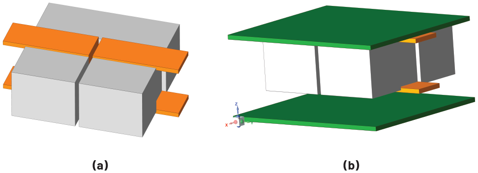
▲그림 1. 시뮬레이션 모델: (a) 구리가 없는 경우, (b) 구리가 있는 경우
■ 와전류 발생과 그에 따른 인덕턴스 감소
FEA 시뮬레이션에서는 하나의 권선에 고주파 AC 자극(excitation)를 인가하고, 다른 권선은 개방 상태(전류 없음)로 두어 자기 인덕턴스(self-inductance), 상호 인덕턴스(mutual inductance), 누설 인덕턴스(leakage inductance)에 대한 와전류의 영향을 각각 관찰할 수 있도록 했다.
그림 2는 코어 위쪽 공기 영역에서의 자속 밀도(B-field) 분포를 보여준다.
그림 2a와 그림 2b는 각각 인접한 구리층이 없는 경우와 구리층이 포함된 경우를 보여준다.
구리는 전기 전도도가 높기 때문에 누설 자속이 구리층을 통과해 위쪽 공기 영역으로 퍼지지 않도록 차단되며, 그 결과 주변 공기 영역에서의 누설 자속이 크게 감소한다.
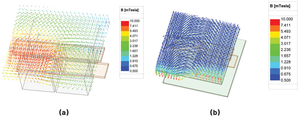
▲그림 2. 코어 위쪽에서의 자속 밀도(B-필드) 분포: (a) 구리가 없는 경우, (b) 구리가 있는 경우
그림 2a의 자속 분포에 오른손 법칙(right-hand rule)을 적용하면, 그림 3에 나타난 것처럼 상부 구리층에 반시계 방향의 와전류가 유도되는 것을 확인할 수 있다.
가장 강한 와전류는 코어의 에어 갭 상부에서 나타나는데, 이는 해당 영역에서 더 많은 자속이 주변 공기 공간으로 누설되기 때문이다.
또한 전류의 발생원에 더 가까운 권선 위쪽에서도 강한 와전류가 발생한다.
.jpg)
▲그림 3. 상부 구리층에서의 와전류 방향과 밀도
그림 4a는 B-필드를 관찰하기 위한 관측 시트(분홍색)를 나타낸 것이다.
그림 4b는 B-필드 분포 그래프로, 누설 자속이 구리층에 의해 억제되는 모습을 보여준다.
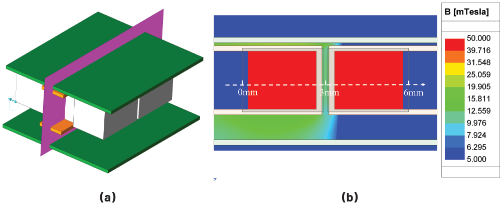
▲그림 4. B-필드 그래프: (a) 관측 평면, (b) 결과
그림 5는 그림 4b에 표시된 코어 중앙의 흰색 점선 경로를 따라 측정한 자속 밀도(B-필드)를 보여준다.
하나의 권선만 여기되었기 때문에, 여기된 권선과 연결된 코어 구간(0 < 거리 < 3 ㎜)에서의 B-필드는 자기 인덕턴스(self-inductance)와 관련한 전체 자속을 나타낸다.
반면, 여기되지 않은 권선과 연결된 구간(3 ㎜ < 거리 < 6 ㎜)에서의 B-필드는 상호 인덕턴스(mutual inductance)와 관련한 상호 자속을 의미한다.
주황색 곡선은 구리층이 있는 경우, 파란색 곡선은 구리층이 없는 경우를 각각 보여준다.
상호 자속은 거의 변하지 않지만, 구리층이 존재할 경우 누설 자속이 감소하기 때문에 전체 자속은 크게 줄어드는 것을 확인할 수 있다.
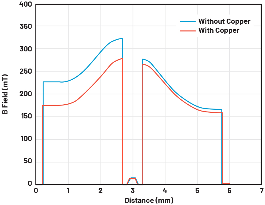
▲그림 5. 코어 내부의 B-필드 분포
구리층과 자기 코어 사이의 거리가 인덕턴스에 미치는 영향을 조사하기 위해, 상부 구리층은 권선 위쪽 100µm 위치에 배치하고 하부 구리층은 권선 아래쪽 900µm 위치에 배치했다.
자기 인덕턴스(L11), 상호 인덕턴스(L12), 누설 인덕턴스(Lk1), 결합 계수(k)를 포함한 시뮬레이션 인덕턴스 값은 하나의 사례를 기준으로 표 1에 정리되어 있다.
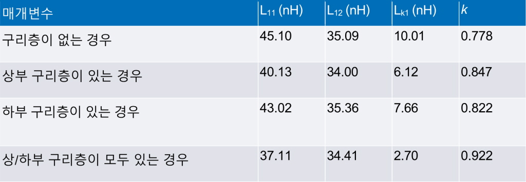
▲표 1. 시뮬레이션 인덕턴스 값
표 1에서 볼 수 있듯이 상부 구리층은 하부 구리층보다 자기 코어와 권선에 더 가까이 위치하기 때문에 누설 인덕턴스와 자기 인덕턴스에 더 큰 영향을 미친다.
두 개의 구리층이 모두 존재할 경우, 자기 인덕턴스는 17.7% 감소하고, 누설 인덕턴스는 73.0% 감소한다.
이렇게 감소한 인덕턴스 값이 듀티비 0.15의 4상 TLVR 기반 벅 컨버터에 적용되면 전류 리플이 최대 50%까지 증가할 수 있다.
그림 3에서 볼 수 있듯이 가장 강한 와전류는 코어의 에어 갭 상부와 여기된 권선 위쪽에서 발생한다.
이러한 와전류가 인덕턴스 변화에 미치는 개별적인 영향을 평가하기 위해, 그림 6과 같이 해당 위치의 구리층에 홈(groove)을 도입했다.
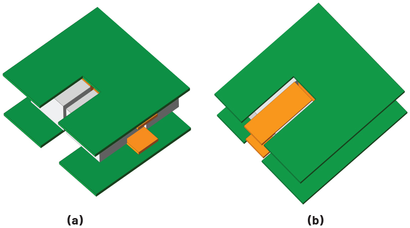
▲그림 6. 홈이 가공된 구리층: (a) 코어 에어 갭 인근, (b) 권선 인근
그림 7은 두 가지 홈 가공 구리층 구성에 대한 B-필드 분포를 보여준다.
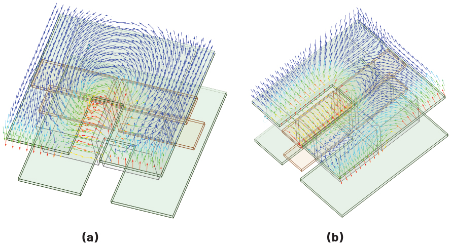
▲그림 7. 홈이 가공된 구리층이 적용된 경우 코어 상부의 자속 밀도(B-필드) 분포: (a) 코어 에어 갭 인근, (b) 권선 인근
그림 7a에서는 두 코어 구간 사이의 쇄교 자속 (flux linkage)이 크게 개선되어 상호 자속이 증가하는데, 이는 표 2에서 확인할 수 있다.
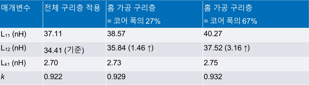
▲표 2. 코어 에어 갭 상부에 홈 가공 구리층을 적용했을 때 시뮬레이션 인덕턴스 값

그림 7b에서는 권선 위쪽 공기 영역으로의 누설 자속(flux leakage)이 현저히 증가하며, 그 결과 누설량이 더 많아짐을 표 3에서 확인할 수 있다.
전체 구리층은 누설 자속을 줄이는 역할을 하기 때문에, 권선 위쪽에만 홈을 추가하는 방식은 제한적인 개선 효과만 제공한다.
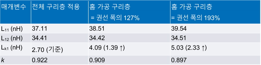
▲표 3. 권선 상부에 홈 가공 구리층을 적용했을 때 시뮬레이션 인덕턴스 값
■ 인접 금속에서 발생하는 와전류 효과 완화 전략
▶ 에어 갭 길이 축소
앞서 언급했듯이 인접 금속에서 발생하는 와전류로 인해 효율이 감소하는 이유는 크게 두 가지다.
첫 번째는 인덕턴스 감소로 인해 전류 리플이 커지는 것이고, 두 번째는 주변 금속 부품에서 발생하는 와전류로 인해 추가 손실이 발생하는 것이다.
인덕턴스를 개선하기 위한 첫 번째 방법은 코어의 에어 갭 길이를 줄이는 것이다.
코어 에어 갭을 줄이면 자기 저항(magnetic reluctance)이 감소하여 더 많은 자속이 형성될 수 있으며, 그 결과 인덕턴스가 증가한다.
또한 자속이 코어 소재 내부에 더 잘 집중되도록 하여 주변 공기 영역으로의 누설 자속을 줄이고, 그에 따라 인접한 도전성 구조에서 발생하는 와전류와 관련 손실을 완화할 수 있다(그림 8).
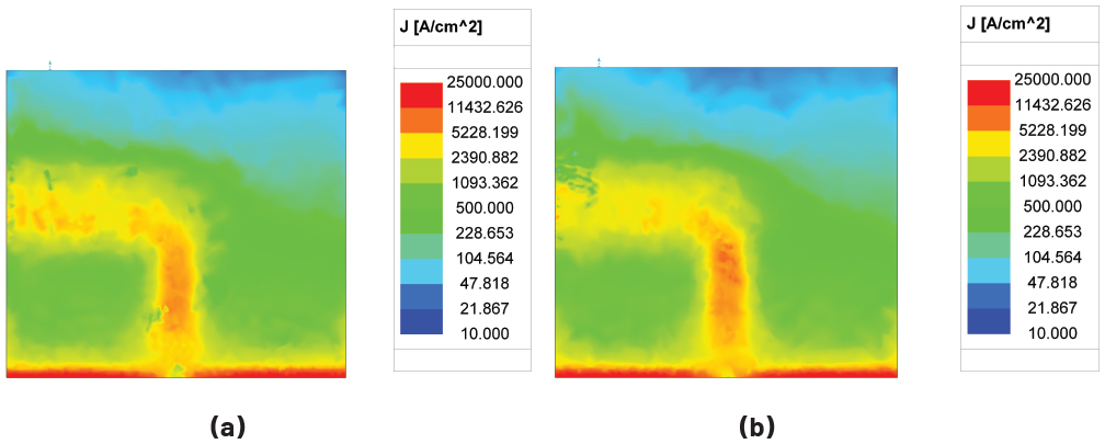
▲그림 8. 상부 구리층에서의 와전류 밀도: (a) (lg = 0.25) ㎜, (b) (lg = 0.15) ㎜
표 4는 서로 다른 두 가지 코어 에어 갭 길이 (lg)에 대해 인덕턴스 값을 비교한 시뮬레이션 결과를 예시한 것이다.
에어 갭이 0.15㎜에서 0.25㎜로 증가하면 전체 인덕턴스는 37.2% 증가하고 상호 인덕턴스는 40.1% 증가한다.
이 방법을 통해 감소되는 와전류 손실은 표 5과 같다. 다만 이러한 방식의 단점은 인덕터의 포화 전류(saturation current)가 낮아질 수 있다는 점이다.
.jpg)
▲표 4. 에어 갭 길이에 따른 시뮬레이션 인덕턴스 값
▶ 지배적인 구리층 제거
인접 도체가 기판 내부의 여러 구리층들인 경우, 와전류 손실을 줄이는 한 가지 방법은 권선과 자기 코어에 가장 가까운 하위층(sublayer)의 구리 면적을 줄이는 것이다.
구리층이 권선에 가까울수록 더 강한 자기 자속을 받게 되며, 그 결과 더 큰 와전류가 유도된다.
예를 들어 그림 9와 같이 상부 기판의 하단 구리층을 제거하는 방법을 적용할 수 있다.
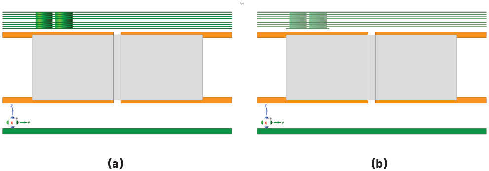
▲그림 9. 기판 내 다층 구리 구조: (a) 8층, (b) 7층
그림 10은 8개의 구리 하위층에서 발생하는 와전류 밀도를 보여준다.
그림에서 볼 수 있듯이 8번 하위층(최하위층)는 가장 강한 와전류를 가지며, 1번 하위층(최상위 레이어)는 가장 약한 와전류를 가진다.
와전류의 방향은 권선에서 발생한 원래의 자기 자속뿐만 아니라 인접한 구리 하위층에서 발생하는 와전류의 영향도 함께 받는다.
구리층이 얇은 경우 권선에서 발생한 자속을 완전히 차단하지 못하기 때문에 일부 자속이 상부층으로 통과해 상위 구리층에서도 와전류를 유도할 수 있다.
반면 구리층이 권선으로부터 충분히 멀리 떨어져 있거나 인접한 하위층이 자속을 차단할 만큼 충분히 두꺼운 경우, 권선에서 발생하는 자속의 영향은 거의 무시할 수 있는 수준이다.
이러한 경우 구리층에서 발생하는 와전류는 주로 인접한 구리층의 전류에 의해 유도된다.
예를 들어 그림 11에서 볼 수 있듯이 권선 바로 위에 위치한 8번 하위층의 구리 영역에서는 와전류가 권선 전류와 반대 방향으로 흐르지만, 4번 하위층에서는 와전류가 권선 전류와 같은 방향으로 흐르게 된다.
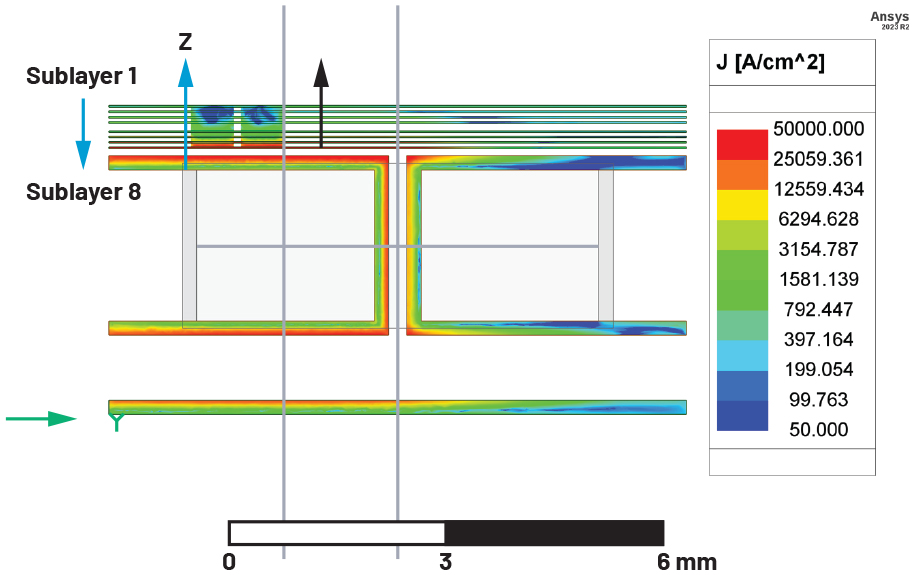
▲그림 10. 구리 하위층에서의 와전류 밀도
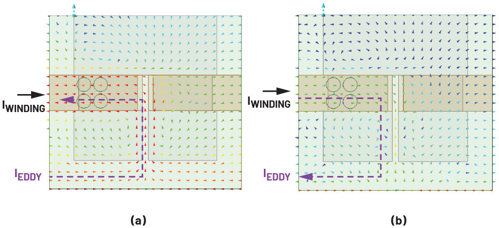
▲그림 11. 와전류 방향: (a) 8번 하위층 8, (b) 4번 하위층
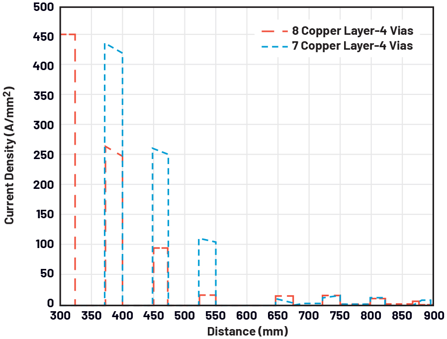
▲그림 12. 와전류 밀도: 8층 구리 하위층 vs. 7층 구리 하위층
그림 12는 그림 10에 표시된 검은 화살표 방향을 따라 측정한 상부 기판의 전류 밀도를 비교한 것이다.
여기서 주황색은 8개의 구리 하위층이 있는 경우를, 파란색은 7개의 구리 하위층이 있는 경우를 나타낸다.
8번 하위층을 제거하면 해당 층에는 구리가 존재하지 않기 때문에 와전류가 0으로 감소하며, 이는 표 5에서 보이는 것처럼 와전류 손실을 줄이는 데 도움이 된다.
그러나 7번, 6번, 5번 하위층의 전류 밀도는 8개의 구리층이 존재하는 경우보다 크게 증가한다.
이는 권선에서 발생하는 자기 자속을 차단하던 8번 하위층이 제거되면서 남아 있는 층들에 강한 와전류가 유도되기 때문이다.
따라서 이 방법은 와전류 손실 감소에는 도움이 되지만 인덕턴스를 증가시키는 데에는 도움이 되지 않는다.
▶ 스위칭 주파수 증가
와전류의 영향을 줄이는 또 다른 방법은 스위칭 주파수를 높이는 것이다.
스위칭 주파수를 높이면 전류 리플이 감소하며, 그 결과 와전류 손실(Peddy)도 줄어든다(표 5). 방법 1, 방법 2, 방법 3을 함께 적용하면 컨버터의 최대 효율은 87.4%에서 89%로 향상되며, 최대 부하(full-load) 효율은 86.7%에서 87.2%로 높아진다.
.jpg)
▲표 5. 다양한 방법 적용 시 금속에서의 와전류 손실(Peddy) 비교
■ 상부 인덕터 에어 갭이 µModule® 레귤레이터 성능에 미치는 영향
LTM4680은 최대 16 VIN을 지원하는 스텝다운 µModule 레귤레이터로, 듀얼 30A 또는 단일 60A 출력을 제공하며 디지털 PMBus® 인터페이스를 갖추고 있다.
이 디바이스는 16㎜ × 16㎜ × 7.82㎜ 크기의 소형 BGA 패키지로 제공된다.
LTM4700은 더 높은 전류 용량을 제공하는 제품으로, 듀얼 50A 또는 단일 100A 출력을 지원하며 15㎜ × 22㎜ × 7.87㎜ 크기의 BGA 패키지로 제공된다.
두 제품 모두 다양한 애플리케이션에서 우수한 성능을 제공하도록 설계됐다. 작은 패키지 크기로 우수한 효율을 구현하기 위해, 에어 갭이 있는 페라이트 코어 인덕터가 패키지 상단에 통합되어 있다.
그림 13은 LTM4700 패키지의 3D 모델을 보여준다.
히트싱크나 추가 PCB가 모듈 상단에 가깝게 배치될 경우, 앞서 설명한 와전류 효과로 인해 인덕턴스와 전체 효율이 감소할 수 있다.
이러한 영향을 줄이기 위해 그림 14와 같이 히트싱크 금속 평면에 홈을 가공하는 방법을 적용할 수 있다.
또한 다층 PCB가 LTM4700 또는 LTM4680의 상단 표면 가까이에 배치되는 경우, 주요 구리층을 제거하면 와전류 손실을 추가로 줄일 수 있다.
대안으로 스위칭 주파수를 높이는 방법도 고려할 수 있지만, 이 경우 스위칭 손실이 증가할 수 있다는 점을 감안해야 한다.
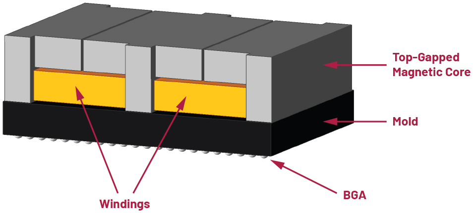
▲그림 13. LTM4700 패키지의 3D 모델
.jpg)
▲그림 14. 와전류 효과를 완화하도록 제안된 홈 가공 히트싱크 구조
■ 결론
이 글에서는 자기 부품이 도전성 소재 근처에 배치될 때 발생하는 와전류로 인해 전력 시스템의 효율이 저하되는 원인을 분석했다.
이러한 유도 전류는 추가적인 손실을 유발할 뿐만 아니라 유효 인덕턴스를 감소시켜 전류 리플 증가와 더 높은 AC 손실을 초래한다.
이러한 현상을 평가하기 위해 유한요소해석(FEA) 시뮬레이션을 수행했다. 효율 개선을 위한 세 가지 완화 전략도 제안됐다.
첫째는 코어 에어 갭의 길이를 줄이는 방법이며, 둘째는 주요 구리 영역을 제거하는 방법, 셋째는 스위칭 주파수를 높이는 방법이다.
코어 에어 갭을 줄이는 방식은 인덕턴스 감소와 와전류 손실을 동시에 해결할 수 있지만, 인덕터의 포화 전류가 낮아질 수 있다는 트레이드오프가 존재한다.
나머지 두 가지 방법은 주로 와전류로 인한 손실을 줄이는 데 초점을 맞춘다.
이 글에서 제시한 내용은 LTM4700과 LTM4680 설계에 적용할 수 있으며, 실제 애플리케이션에서 와전류가 발생하는 경우 다양한 전략을 활용해 그 영향을 완화할 수 있다.
※ 저자 소개
민 가오(Min Gao)는 제품 애플리케이션 담당 선임 엔지니어로, 미국 플로리다주 탈라하시에 위치한 플로리다 주립대학교에서 전기공학 박사 학위를 취득했다. 이후 2025년 캘리포니아에서 아나로그디바이스(Analog Devices)에 애플리케이션 엔지니어로 합류했다.
YT 탕(YT (Ye) Tang)은 제품 애플리케이션 담당 스태프 엔지니어로, 2021년 2월 아나로그 디바이스에 합류했다. 현재 µModule® 그룹에서 설계 엔지니어 및 애플리케이션 엔지니어로 근무하며 데이터센터, 광통신 및 다양한 시장을 위한 고출력 전류 POL(point-of-load) 컨버터를 개발하고 있다. 또한 최신 FET와 결합 인덕터 기술을 활용해 POL 스위칭 전원공급장치의 크기를 줄이고 전력 밀도를 높이는 연구에 집중하고 있다.
링 장(Ling Jiang)은 제품 애플리케이션 담당 선임 매니저이다. 2018년 미국 테네시주 녹스빌에 위치한 테네시대학교에서 전기공학 박사 학위를 취득했다. 졸업 후 캘리포니아 베이 지역의 아나로그디바이스 전력 제품 그룹에 합류했으며, 현재 다양한 시장 애플리케이션을 위한 µModule® 제품을 지원하는 선임 매니저로 활동하고 있다. 또한 고밀도 µModule 레귤레이터의 정의와 설계에도 기여하고 있다.
Comments
Related news

ADI Innovates AI Embedded Development and Upgrades Open-Source Development Platform
Global semiconductor company Analog Devices, Inc. (ADI) has officially announced 'CodeFusion Studio™ 2.0,' a major upgrade to its open-source embedded development platform. This update focuses on simplifying and accelerating AI-based embedded systems development while providing a developer-centric integrated toolchain.
2025.11.04by 명세환 기자
ADI, “Simple and Efficient Voltage Inverting Possible Without 'LTC7899' Transformer”
We spoke with Frederik Dostal, power management expert at Analog Devices, Inc., about voltage conversion ICs in inverting topology.
2025.11.06by 명세환 기자
.jpg)
ADI, “Overvoltage Safety Protection with ‘LT4363’ MOSFET SOA Precision Management”
We spoke with Frederik Dostal, a power management expert at Analog Devices, Inc., about how to easily offset overvoltage using protection circuits.
2025.12.05by 명세환 기자
[Technical Contribution] ADI Develops Scalable Beamforming Engine for Quad-Apollo MxFE Radar and Communications Systems
We spoke with Siddhartha Das, System Applications Engineer at Analog Devices, Inc., about how Analog Devices' Apollo MxFE-based digital beamforming platform implements a phase-coherent, scalable direct RF sampling architecture for next-generation radar and communication systems.
2026.01.12by 명세환 기자
.jpg)
In AI accelerator power design, 'endurance structure' is now the competitive edge.
As AI accelerator performance competition intensifies, the focus of server design is shifting toward power delivery. The latest AI accelerators require thousands of amperes of current in nanosecond intervals at low voltages, making power supplies not merely a source but a subject of dynamic control. Macnica FAE Jeongpil Hwang explains that multiphase power architecture is essential in this environment. The differences between PCIe and OAM platforms further complicate power, thermal, and layout requirements. ADI's AI Power Solution is gaining attention as a practical power design alternative for AI server developers by reducing current ripple and lowering design risk through coupled inductors and design tools and guides.
2026.01.23by 명세환 기자











