


SEMI: “Semiconductor materials market reaches $73.2 billion… all-time high”
 Published2026.05.13 15:10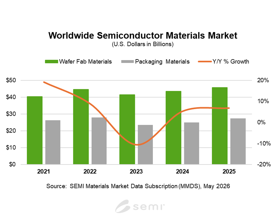
Wafer fabs and packaging materials grow alongside expanding demand for AI and HBM
SEMI announced the results of its 2025 global semiconductor materials market survey on the 13th. It was found that rising process complexity, expanding demand for advanced nodes, and investments in high-performance computing and memory manufacturing have driven up demand for both wafer fabs and packaging materials.
Wafer fab materials revenue reached $45.8 billion, up 5.4% from the previous year. Lithography-related materials, such as photomasks, photoresists, and auxiliary materials, as well as wet chemicals, recorded double-digit growth rates. This is due to higher requirements for the photolithography process and an increase in process steps resulting from the transition to advanced processes.
Sales of packaging materials increased by 9.3% to $27.4 billion. Substrates and bonding wires led the growth. Substrates were affected by the expansion of demand for advanced packaging, while rising gold prices acted as a factor in sales growth for bonding wires.
By region, Taiwan maintained its position as the world's largest consumer of semiconductor materials for the 16th consecutive year with $21.7 billion. China ranked second with $15.6 billion, showing double-digit growth, while South Korea recorded $11.2 billion. Year-on-year growth was observed in all regions except Europe, with China and North America showing the highest growth rates among major regions.
These statistics are based on SEMI's Materials Market Data Subscription (MMDS). MMDS provides annual sales data, 10 years of historical data, and a 2-year forecast, and includes data for seven regions, including North America, Europe, Japan, Taiwan, Korea, and China.
The growth trend in the semiconductor materials market demonstrates that increased investment centered on AI and HBM is driving demand for materials. As competition in advanced processes and cutting-edge packaging continues, the materials market is becoming an indicator reflecting both the semiconductor market recovery and technological transformation.

Comments
Related news
Semiconductor equipment investment in 2024 to reach $117.1 billion, up 10% from the previous year
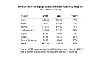
According to SEMI, an industry association representing the global electronics industry supply chain, semiconductor manufacturing equipment investment reached $117.1 billion in 2024, representing a 10% increase compared to the previous year. The global semiconductor equipment market in 2024 achieved a record high due to various factors including increased demand for AI and high-performance computing and changes in investment policies by country.
2025.05.27by 명세환 기자
.jpg)
Semiconductor safety standard 'SEMI S2' published in Korean, with experts from Samsung and SK Hynix participating to accelerate field implementation.
The Semiconductor Equipment and Materials International (SEMI) has translated the revised SEMI S2-0724, a key safety standard for the global semiconductor industry, into Korean, and it is expected to enable the immediate application of the latest safety standards in all fields of semiconductor manufacturing equipment design and safety evaluation.
2025.07.03by 배종인 기자
AI Demand Surges, Semiconductor Production Capacity Increases 69%
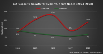
According to SEMI's "300mm Fab Outlook Report," which represents the global electronics industry supply chain, global wafer production capacity is expected to grow at an average annual rate of 7% from the end of 2024 through 2028, with monthly production volumes reaching 11.1 million wafers per month (Wpm) by 2028. In particular, advanced process wafers of 7 nanometers and below are projected to surge approximately 69% from 850,000 wafers in 2024 to 1.4 million wafers in 2028. This represents an average annual growth rate of 14%, which is double the industry average overall.
2025.07.11by 배종인 기자
Demand for semiconductor equipment continues to grow
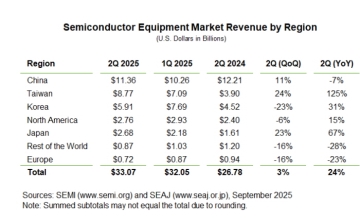
According to the latest report from SEMI (Semiconductor Equipment and Materials International), global semiconductor equipment sales in the second quarter of 2025 reached $33.07 billion, representing a 24% increase compared to the same period of the previous year.
2025.10.15by 명세환 기자
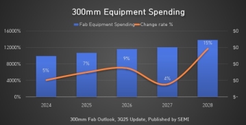
Korea Ranks 2nd in 300mm Fab Equipment Investment by 2028
According to the latest "300mm Fab Outlook Report" released by SEMI, an industry association representing the global electronics industry supply chain, worldwide 300mm fab equipment investment is projected to reach a total of $374 billion from 2026 through 2028.
2025.10.27by 명세환 기자











