


This page was machine-translated and may differ from the original. View original
ADI, “Innovation to Simplify Power Compensation Evaluation Using Software-Based Compensation Probes”
 Published2026.05.19 10:19
전원공급장치 제어 루프 보상값 빠르게 변경·검증, 품질·효율 동시 향상
더 우수한 전원공급장치 설계 가능, 설계 시간을 단축하는 데에도 기여
더 우수한 전원공급장치 설계 가능, 설계 시간을 단축하는 데에도 기여
■ 개요
이 글에서는 전원공급장치가 레귤레이션 루프를 포함하고 있는 이유와, 최상의 성능을 달성하기 위해 이들 루프를 최적화하는 방법에 대해 설명한다.
설계 과정이 실제로 정확하게 이루어졌는지를 확인하기 위해서는 성능 시험이 실험실에서 반드시 진행되어야 한다.
이러한 실험실 작업은 보상 부품을 조정하기 위해 서로 다른 값의 커패시터와 저항을 납땜하는 절차가 포함해야 하므로 많은 시간이 소요된다.
소프트웨어로 제어되는 보상 프로브 카드를 사용하면 이러한 납땜 작업을 마우스 클릭으로 대체할 수 있어, 작업 부담을 줄이고 평가 시간을 단축할 수 있다.
■ 머리말
전원공급장치는 일반적으로 고정된 출력 전압을 생성하도록 설계된다.
이 출력 전압은 발진하지 않아야 하며, 부하 과도 응답이나 입력 전압의 변동에도 불구하고 일정하게 유지되어야 한다.
스위치 모드 전원공급장치(SMPS)의 제어 루프를 최적화하기 위해, 많은 전원공급 IC에는 보상 핀이 포함되어 있다.
이러한 핀은 적절한 보상 부품, 즉 커패시터와 저항을 연결함으로써 제어 루프를 최적화할 수 있으며, 루프 안정성을 유지하면서 가능한 한 높은 제어 대역폭을 달성하도록 한다.
제어 루프를 조정할 수 있도록 한 이유는 동작 조건과 전원 경로에 사용되는 외부 부품의 선택에 따라 보상 방식이 달라져야 하기 때문이다.
그림 1은 보상 핀 VC를 갖는 벅(스텝다운) 레귤레이터를 보여준다.
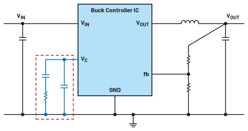
▲그림 1. 제어 루프 속도와 안정성을 조정하기 위한 보상 부품(파란색)을 포함하고 있는 스위치 모드 전원공급장치
AD

보상 부품의 선택은 LTpowerCAD®나 LTspice®와 같은 적절한 계산 및 시뮬레이션 프로그램을 통해 수행할 수 있다.
그러나 회로 기판 레이아웃의 기생 효과도 일정 부분 영향을 미친다. 따라서 전원공급장치는 항상 실제 하드웨어에서 검증되어야 하며, 이 과정에서 보상 부품의 선택이 최종적으로 확인 및 검증된다.
전원공급장치 설계 과정에서 이러한 단계는 많은 시간이 소요된다.
예를 들어, LTpowerAnalyzer를 사용하여 보드 다이어그램(Bode diagram)이나 부하 과도 응답 측정을 수행해야 한다.
만약 얻어진 결과가 설계 목표를 충족하지 못하면, 이를 최적화해야 한다.
이를 위해 기존 보상 부품을 제거하고 다른 값의 부품을 다시 납땜해야 하는데, 이러한 과정은 손이 많이 가고 시간도 많이 걸린다.
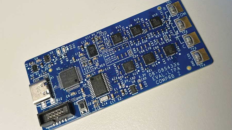
▲그림 2. GUI를 이용해 보상 핀의 다양한 설정을 최단 시간에 실행할 수 있는 EVAL-LTPA-COMPRB 평가 보드
그림 2는 아나로그디바이스(Analog Devices)가 제공하는 평가 보드로, 보상 프로브(compensation probe)라고 불린다.
이 카드는 오른쪽의 솔더 접점을 통해 어떠한 전원공급장치의 보상 핀이나 접지 핀에든 연결할 수 있다.
이 보드는 그림 1의 빨간색 사각형에 표시된 보상 부품을 대체한다.
보드의 왼쪽은 USB 케이블을 통해 PC와 연결된다. 하드웨어 연결을 마쳤으면 LTpowerAnalyzer용 무료 소프트웨어를 실행한다.
이 소프트웨어를 활용하면 다양한 보상 값을 가진 부품들을 그래픽 사용자 인터페이스(GUI)를 이용해 매우 빠르게 전환할 수 있다.
LTpowerAnalyzer를 활용해 보드 다이어그램(Bode diagram)을 생성할 수도 있으며, 서로 다른 보상 설정에서 부하 과도 테스트도 수행할 수 있다.
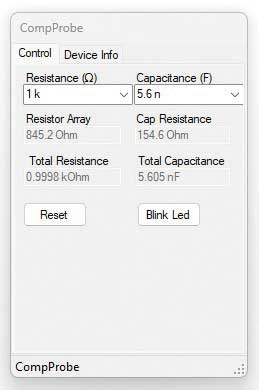
▲그림 3. GUI를 활용한 보상 부품 선택
그림 3은 EVAL-LTPA-COMPRB(보상 프로브) 보드의 소프트웨어 인터페이스를 보여준다.
여기에서는 511Ω∼100kΩ까지의 저항 값과 5pF∼39nF까지의 커패시터 값을 선택할 수 있다.
또한 커패시터의 내부 직렬 저항도 표시되며, 함께 고려할 수도 있다.
이 보상 보드를 테스트 하고자 하는 전원 컨버터 IC의 접지 단자와 보상 핀에 짧은 연결 리드로 연결하면, 다양한 보상 부품 값을 정확하고 간편하며 신속하게 선택할 수 있다.
■ 결론
EVAL-LTPA-COMPRB와 같은 보상 프로브를 사용하면 전원공급장치의 제어 루프 안정성 검증 및 최적화 작업을 매우 손쉽고 효율적으로 수행할 수 있다.
다양한 보상 설정을 매우 짧은 시간 내에 테스트할 수 있는데, 이는 더 우수한 전원공급장치 설계를 가능하게 할 뿐만 아니라 설계 시간을 단축하는 데에도 기여한다.
※ 저자 소개
 프레데릭 도스탈(Frederik Dostal)은 20년 이상의 경력을 보유한 전원 관리 분야 전문가다. 독일 에를랑겐대학교(University of Erlangen)에서 마이크로일렉트로닉스를 전공한 후, 2001년 내셔널 세미컨덕터(National Semiconductor)에 입사해 필드 애플리케이션 엔지니어로 활동하며 고객 프로젝트에서 전력 관리 솔루션을 구현하는 경험을 쌓았다. NS 재직 시 애리조나주 피닉스에서 4년 간 근무하면서 애플리케이션 엔지니어로서 스위치 모드 전원공급장치(SMPS)를 맡았다. 2009년 아나로그 디바이스(Analog Devices)에 합류한 이후에는 제품 라인과 유럽 기술 지원 등 다양한 역할을 수행했으며, 현재는 폭넓은 설계 및 애플리케이션 경험을 바탕으로 전력 관리 전문가로 활동하고 있다. 현재는 아나로그디바이스 뮌헨 지사에서 근무하고 있다.
To request a correction, reply or follow-up report on this article, see how to file a request. Previously published statements are collected in corrections & replies.
Comments
Related news

[Technical Contribution] ADI Frederic Dostal - How to Miniaturize Power Supplies
Analog Devices' Frederik Dostal discusses the miniaturization of power supply units.
2022.07.12by 명세환 기자

[Technical Contribution] ADI Frederic Dostal – Dynamic Control Method for Optimal Output Voltage
Let's hear from Frederik Dostal, FAE at Analog Devices, Inc., about the dynamic adjustment method for appropriate output voltage.
2022.12.06by 명세환 기자

[Technical Contribution] ADI's Frederik Dostal: Designing More Compact Power Supplies with Just One Inductor
We spoke with Frederick Dostal of ADI about methods for designing more compact power supplies using just a single inductor.
2023.03.14by 명세환 기자
.jpg)
[Technical Contribution] ADI's Frederic Dostal: Why Smaller is Better
We heard from Frederick Dostal of Analog Devices (ADI) about the advantages of integrated inductor power modules.
2023.05.22by 명세환 기자
.jpg)
ADI Frederik Dostal, “Power Management Development Toolchain, Architecture Optimization Most Important”
We spoke with Frederick Dostal from Analog Devices (ADI) about the toolchain for developing power management systems.
2024.12.06by 배종인 기자












Sponsored Company