


EVG Supports Resolution of CPO Manufacturing Challenges for AI Data Centers
 Published2026.09.02 11:27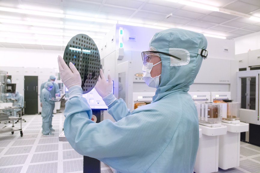
공정 개발부터 대량생산(HVM)까지 제조 밸류체인 전 단계를 포괄한다는 방침이다.
CPO는 광자 집적회로(PIC)·레이저·광학 구조를 동일 패키지에 통합해 광 I/O를 컴퓨팅 소자에 근접 배치하는 방식이다.

구성 소재마다 물리적·제조 특성이 달라 집적 밀도가 높아질수록 새로운 공정 기술이 요구된다.
△하이브리드 본딩: PIC와 전자 집적회로(EIC) 간 기생 효과를 최소화하며 고밀도 집적 구현 △퓨전 본딩: 박막 리튬 나이오베이트(TFLN)·티탄산바륨(BTO) 등 차세대 광 변조 소재 이종 집적 지원 △상온 본딩: 광 손실이 적은 인터페이스 형성 및 다이아몬드·SiC 히트 스프레더 집적을 통한 열 관리 △NIL: 격자 결합기·빔 성형 소자 등 면외 광 결합 소자의 확장 가능한 제조 △임시 본딩·디본딩: 레이저 다이오드 제조 및 첨단 패키징용 웨이퍼 박형화 공정 지원.

Comments
Related news

EVG Announces New NanoCleave Layer Release Technology
EV Group, a leading provider of wafer bonding and lithography equipment for MEMS, nanotechnology, and semiconductor markets, has achieved thin-film 3D stacking from advanced packaging to transistor miniaturization through EVG's innovative layer separation technology utilizing infrared (IR) lasers.
2024.02.01by 배종인 기자

EVG Responds to Future Chip Stacking Needs
EV Group (EVG), providing innovative process solutions and expertise in advanced semiconductor design and chip integration methods, will present technologies addressing future requirements for chip stacking through Semicon Korea 2025.
2025.02.18by 배종인 기자
EV Group Leads Innovation in 300㎜ MEMS Manufacturing Technology
EV Group (EVG), a leading company in advanced semiconductor manufacturing and chip integration technology, has announced the next-generation GEMINI® automated wafer bonding system for 300 mm wafer manufacturing, and is garnering expectations that it will significantly improve bonding quality and yield of MEMS (Micro-Electro-Mechanical Systems) devices manufactured on large-format wafers.
2025.03.19by 배종인 기자
EVG Unveils Advanced Memory and Packaging Process Solutions at Semicon Korea 2026
EV Group (EVG) will participate in 'Semicon Korea 2026' held at Seoul COEX from February 11 to 13, showcasing key process technologies for advanced memory semiconductors and next-generation packaging.
2026.02.10by 배종인 기자
.jpg)
EVG Unveils Next-Generation EVG®120 for Mass Production… 40% Improved Throughput and 20% Reduced Installation Footspace
EV Group (EVG) has unveiled the next-generation EVG®120 automatic resist processing system targeting mass production environments. The new platform increases throughput by 40% compared to the previous generation, reduces installation footprint by more than 20%, and newly incorporates in-situ resist thickness measurement and wafer edge exposure (WEE) functionality. While inheriting design elements verified in the EVG®150, it supports flexible modular configurations based on a compact footprint. It is characterized by targeting diverse application areas including MEMS, advanced packaging, photonics, and power semiconductors.
2026.02.19by 명세환 기자











