



Samsung Electronics Expands High NA EUV and 12-inch Mask Collaboration with ASML
 Published2026.09.08 15:47
2028년 D램 제조에 High NA EUV 첫 적용 목표
현재 업계는 6인치 마스크를 표준으로 사용하고 있으나, 이를 12인치로 전환하면 패턴을 분할 노광한 뒤 이어붙이는 스티칭(stitching) 제약이 해소돼 팹 생산성 향상과 칩 제조 비용 절감이 가능하다고 회사 측은 설명했다.
수백억 개의 트랜지스터를 집적하는 첨단 반도체일수록 12인치 마스크를 통해 High NA EUV 설비의 성능을 온전히 활용할 수 있다는 것이다.
삼성전자는 컨소시엄 내에서 공동 연구 및 표준 개발 활동에 참여할 계획이다.

High NA EUV는 기존 EUV 대비 개구수(NA)를 높여 더 정밀한 패터닝이 가능한 차세대 노광 기술이다.
양사는 이 기술의 메모리 공정 적용을 통해 D램 미세화 로드맵 연장과 공정 단순화를 동시에 달성할 수 있을 것으로 보고 있다.
파운드리 공정에 이어 메모리 분야로도 High NA EUV 적용 범위가 확대되는 것이다.
크리스토프 푸케 ASML CEO는 “AI가 이끄는 새로운 시대를 맞이해 삼성전자와 함께 차세대 반도체 제조를 위한 혁신을 이끌어 가기를 기대한다”고 밝혔다.

Comments
Related news
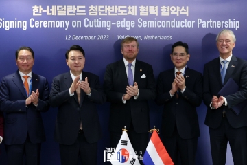
ASML and Samsung Electronics to Invest 1 Trillion Won in Establishing Next-Generation Semiconductor Manufacturing Technology R&D Center in Korea
With the semiconductor industry entering the 3-nanometer era, fierce competition is intensifying in ultra-fine process technology for developing 2-1 nanometer products expected to emerge after 2025. Samsung Electronics has strengthened R&D investments through collaboration with ASML.
2023.12.13by 명세환 기자
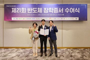
ASM Participates in Semiconductor Scholarship Program for Fifth Consecutive Year…Supporting Science and Engineering Talent
ASM, a semiconductor deposition equipment specialist, participated in the "21st Semiconductor Scholarship Certificate Presentation Ceremony" organized by the Korea Semiconductor Industry Association and presented scholarship certificates to graduate students at Ulsan National Institute of Science and Technology. ASM has been supporting the KSIA scholarship program for five consecutive years since 2022 and is currently conducting multilayered talent development activities including donations to the Hwaseong City Foundation, global exploration programs, and mentoring for women in science and engineering.
2026.10.23by 배종인 기자
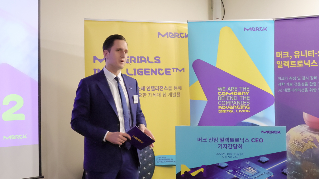
Benjamin Hein, Merck Electronics CEO: "AI is a systems battle, moving beyond materials to integrated workflow"
Benjamin Hein, CEO of Merck Electronics, stated that in the AI era, semiconductor competitiveness depends on system-wide optimization rather than individual components, and announced plans to transform Merck from a materials supplier into an integrated workflow solution company. He identified advanced packaging and semiconductors for AI as key growth drivers, describing advanced packaging as "a high-speed train that has already departed." He also announced plans to focus on front-end processes, advanced packaging, and quantum and neuromorphic computing, while expanding business areas to include software-based yield optimization. He evaluated South Korea as one of Merck's top three global markets with significant growth expected over the next five years.
2026.10.22by 배종인 기자
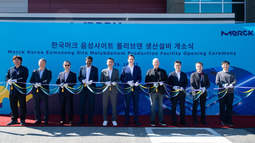
Merck Supports Next-Generation Semiconductor Innovation with Advanced Materials and Supply Technology…Opens Molybdenum Production Facility in Eumseong
Merck has established molybdenum precursor (MoO₂Cl₂) production equipment for next-generation semiconductors at its Eumseong business site in North Chungcheong and has begun full-scale operations. The company's strategy is to enhance semiconductor customers' productivity and supply stability through an integrated solution that combines material production capabilities in Eumseong with the CK VAPOR supply system in Ansan. In response to increased demand for high-performance semiconductors in the AI era, the company plans to supply advanced materials applicable to 3D NAND, DRAM, and logic processes locally and actively support semiconductor innovation in Korea and Asia.
2026.10.22by 배종인 기자
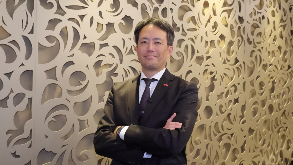
[Interview] Choi Jun-ho, Vice President of Keysight Technologies, "Supporting Advanced Technology Development Through Collaboration and Talent Behind the Frontline of Technology"
Keysight Technologies is leading technological innovation through a platform strategy that integrates design, simulation, emulation, and testing in line with the era of advanced technologies such as AI, data centers, and optical communications. Furthermore, the company is concentrating on enhancing customers' development efficiency and maximizing product utilization by leveraging AI. In addition, to support these efforts, Keysight is actively investing in cultivating talent with cross-domain competencies, engineer education, and strengthening collaboration with customers. In this context, Keysight held the 'Keysight World Tech Day Seoul 2026' on the 21st and introduced the company's advanced technological capabilities. Accordingly, this publication conducted an interview with Choi Jun-ho, Vice President of Keysight Technologies headquarters, at the Keysight World venue to discuss Keysight's advanced technologies and the company's philosophy for supporting advanced technology development.
2026.10.22by 배종인 기자











